Method of manufacturing image display unit, and image display unit

a technology of image display unit and display unit, which is applied in the direction of discharge tube luminescnet screen, tube with screen, and application of light-emitting coatings, etc., can solve the problems of defect not being allowed, damage or destruction of electron emission elements of cathode and fluorescent plane of anode, and limited clearance between front-side substrate and back-side substrate of fed, etc., to achieve high productivity and quality, the effect of low cos

Inactive Publication Date: 2007-08-09
KK TOSHIBA
View PDF3 Cites 3 Cited by
  • Summary
  • Abstract
  • Description
  • Claims
  • Application Information

AI Technical Summary

Benefits of technology

[0011] It is an object of the present invention to provide a method of manufacturing an image display unit with high productivity and quality at low cost, while controlling a surface discharge between metal back films, and an image display unit manufactured by the method.
[0016] A metal back layer is formed just like covering the top face of a fluorescent layer, but not formed on a sidewall of a fluorescent layer. Therefore, conduction between adjacent fluorescent layer patterns is prevented in a state that a film is being formed without using a dividing step after a film is formed, and an electric discharge can be effectively prevented. The width of a vertical partition line dividing rectangular or rectangular strip shaped fluorescent pixels is 20-50 μm, and the width of a horizontal partition line (stripe) is 50-300 μm. These widths of vertical and horizontal partition lines indicate intervals at the bottom of a fluorescent layer regardless of a sectional form (rectangular, trapezoidal, inverse trapezoidal) of a fluorescent layer.

Problems solved by technology

However, a clearance between a front-side substrate and a back-side substrate of FED is limited from the viewpoint of resolution and characteristics of a support member, and needs to be set to 1-2 mm.
Once an electric discharge occurs, a large discharge current of several amperes to several hundreds amperes flows in a moment, and an electron emission element of a cathode and a fluorescent plane of an anode may be damaged or destroyed.
Such an electric discharge causing a defect should not be allowed as a product.
However, in the above prior art, a process of dividing a formed metal back film is necessary, and productivity is decreased and cost is increased.
Further, in a process of dividing a metal back film, there is a possibility that a fluorescent layer as a base layer is damaged.

Method used


Image

  • Method of manufacturing image display unit, and image display unit
  • Method of manufacturing image display unit, and image display unit
  • Method of manufacturing image display unit, and image display unit

Examples


embodiment 1

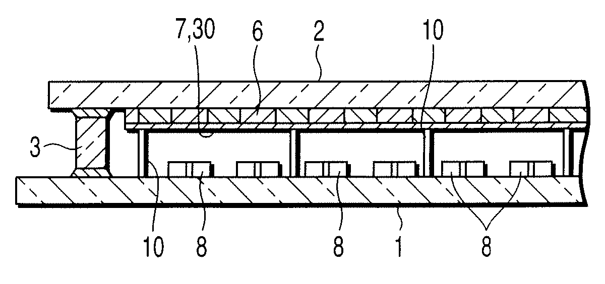
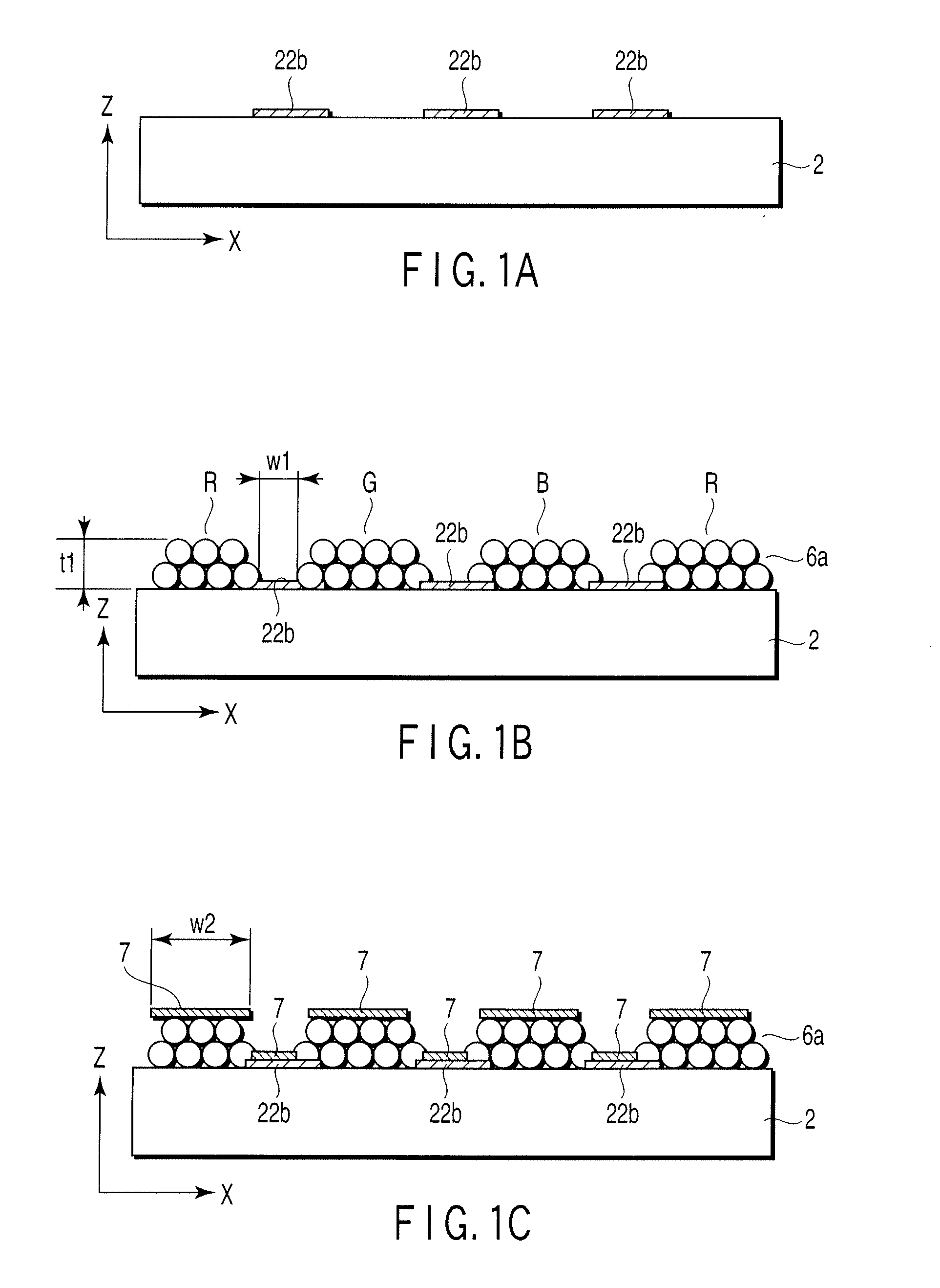
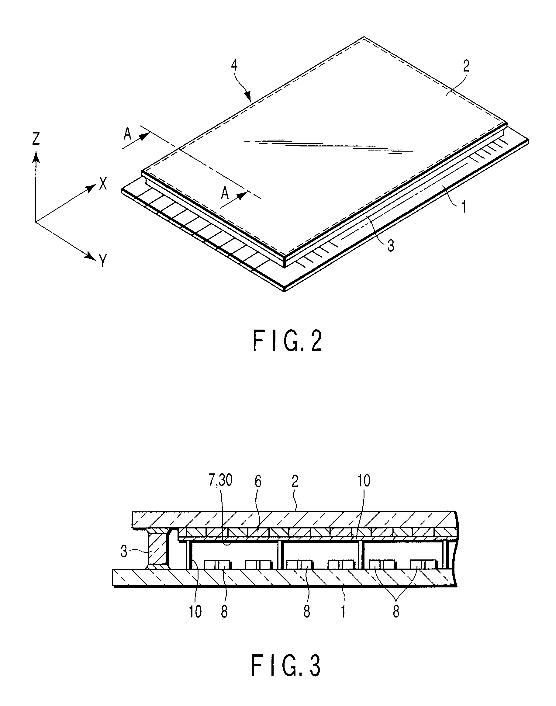
[0047] A matrix pattern of light-shielding layers made of black pigment is formed on a glass substrate by photolithography. A fluorescent layer with a rectangular repetitive pattern of red (R), green (G) and blue (B) is formed in the space among the matrix pattern of light-shielding layers by patterning by photolithography by using Y2O2S:Eu3+ as a red (R) fluorescent body, ZnS:Cu, as a green (G) fluorescent body, and ZnS:Ag as a blue (B) fluorescent body. Finally, the substrate 2 is baked to eliminate a photoresist, and obtain a fluorescent plane with a 3-color pattern of fluorescent layers arranged regularly in the vertical and horizontal directions. A square pixel with a pitch of 600 μm is formed on the fluorescent plane, and the width W1 of the fluorescent layer in the X direction of a vertical partition line is 30 μm.

[0048] A metal back layer made of an Al film is formed on the top face of the obtained 3-color pattern of fluorescent layers by vacuum evaporation. Namely, form an...

embodiment 2

[0053] A repetitive pattern of fluorescent layers of red (R), green (G) and blue (B) is formed in the space among the light-shielding layers of a matrix pattern formed as in the embodiment 1, by patterning by photolithography by using YVO4:Eu3+ as a red (R) fluorescent body, (Zn, Cd)S:Cu as a green (G) fluorescent body, and ZnS:Ag as a blue (B) fluorescent body. A square pixel with a pitch of 600 μm is formed on the fluorescent plane, and the width W1 of the fluorescent layer in the X direction of a vertical partition line is 20 μm.

[0054] A metal back layer to be provided on the top face of the fluorescent layer is formed under the same conditions of the embodiment 1. FED is made by executing a post-process under the same conditions as the embodiment 1.

[0055] Electric breakdown between patterns (surface discharge between metal back layers) in FED obtained by the embodiment 2 is examined, and a good result is obtained.


PUM


Abstract

A method of manufacturing an image display unit comprising forming a light-shielding layer by patterning on a front-side substrate opposed to a back-side substrate on which a number of electron emission elements are arranged, forming a plurality of fluorescent layer as a discontinuous pattern at intervals in an area where the light-shielding layer does not exist, and forming a metal back layer having an anode function on a top face of the fluorescent layer.

Description

CROSS-REFERENCE TO RELATED APPLICATIONS [0001] This is a Continuation Application of PCT Application No. PCT / JP2005 / 014035, filed Aug. 1, 2005, which was published under PCT Article 21(2) in Japanese. [0002] This application is based upon and claims the benefit of priority from prior Japanese Patent Application No. 2004-226918, filed Aug. 3, 2004, the entire contents of which are incorporated herein by reference.BACKGROUND OF THE INVENTION [0003] 1. Field of the Invention [0004] The present invention relates to a method of manufacturing an image display unit, and an image display unit. In particular, the invention relates to a method of manufacturing a flat image display unit using an electron emission element. [0005] 2. Description of the Related Art [0006] A flat image display unit has been developed as a next-generation image display unit in recent years. In the flat image display unit, a number of electron emission elements are arranged to be opposite to a fluorescent plane. An ...

Claims


Application Information

Patent Timeline
Patent Type & Authority Applications(United States)
IPC IPC(8): H01J63/04
CPCH01J9/148H01J29/085H01J29/28H01J2329/323H01J31/127H01J2329/08H01J2329/28H01J29/327H01J9/20H01J9/22H01J31/12
Inventor NAKAMURA, AKIYOSHIKOZUKA, TOMOKOMIKAMI, AKIRAITO, TAKEO
Owner KK TOSHIBA
Why Eureka
Try Eureka