Power amplifier bias protection for depletion mode transistor

a power amplifier and transistor technology, applied in amplifiers, amplifier protection circuit arrangements, electrical devices, etc., can solve the problems of severe constraints on ldmos technology, difficult or impossible to achieve rf power, and broad/wideband performance, and achieve cost-effective effects

Inactive Publication Date: 2007-08-09
ALCATEL LUCENT SAS
View PDF5 Cites 7 Cited by
  • Summary
  • Abstract
  • Description
  • Claims
  • Application Information

AI Technical Summary

Benefits of technology

[0010]In view of the above, it is an object of the present invention to provide an amplifier suitable for broad-, wide- & multiband power amplifier applications while being also cost effective amongst others by being robust to usual current electrical disturbance.

Problems solved by technology

The problem lies with current silicon-based Laterally Diffused Metal Oxide Silicon LDMOS RF power transistors—which often form the basis of power amplifiers.
By use of LDMOS-based power amplifiers, it is very difficult or impossible to achieve RF power i.e. broad- / wideband performance efficiently at the signal purity levels required for cost- and capacity-effective 2.5 G and 3 G multiband / multistandard applications
These requirements place severe constraints on LDMOS technology.
Disregarding this sequence will cause damage or defect to the power transistor, since its channel is open and the device consumes much too high current
However, its ability to continue addressing this market in next generation systems is questionable due to its operating frequency, breakdown voltage, power density and bandwidth limitations.

Method used


Image

  • Power amplifier bias protection for depletion mode transistor
  • Power amplifier bias protection for depletion mode transistor
  • Power amplifier bias protection for depletion mode transistor

Examples


Embodiment Construction

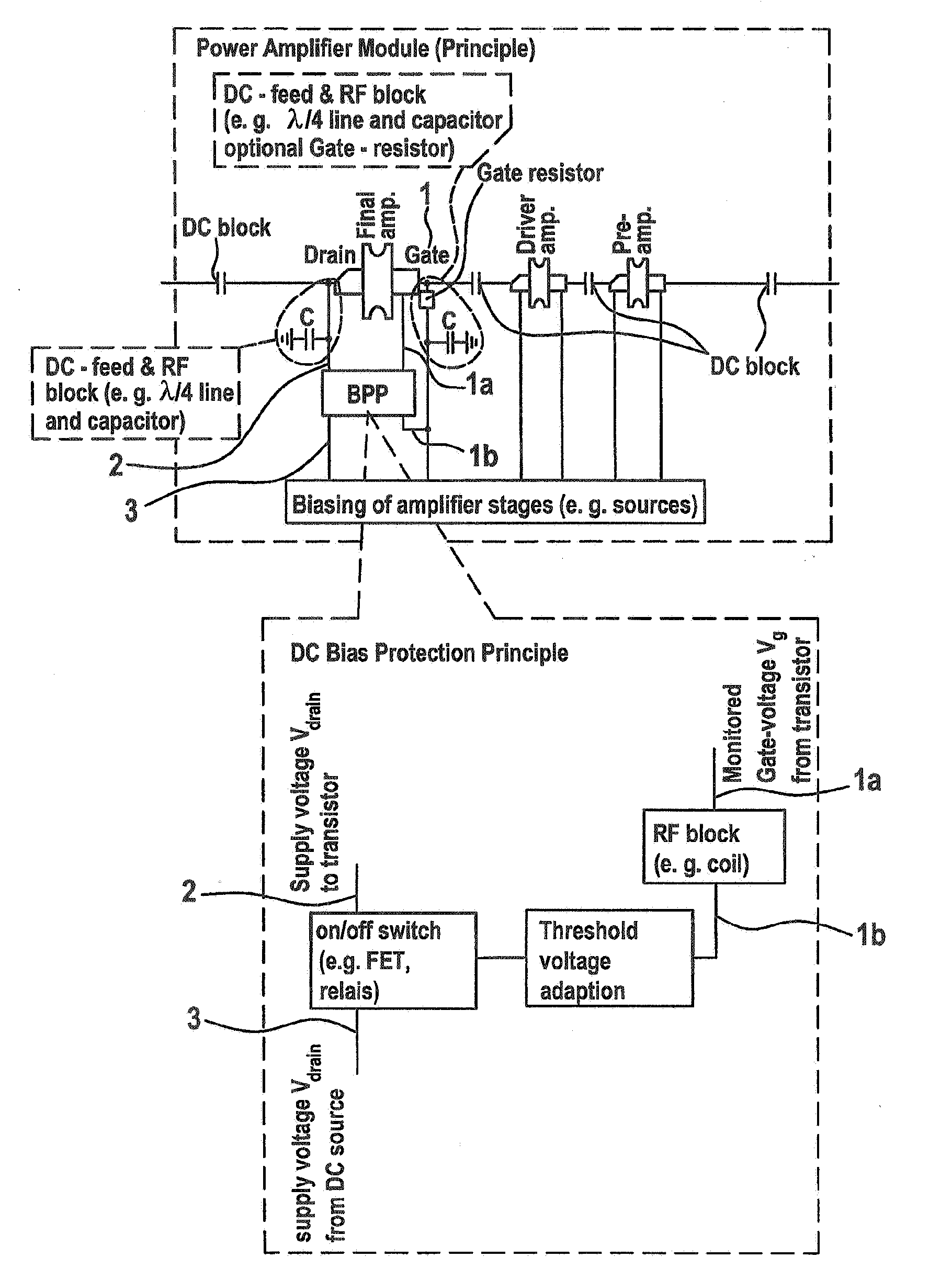
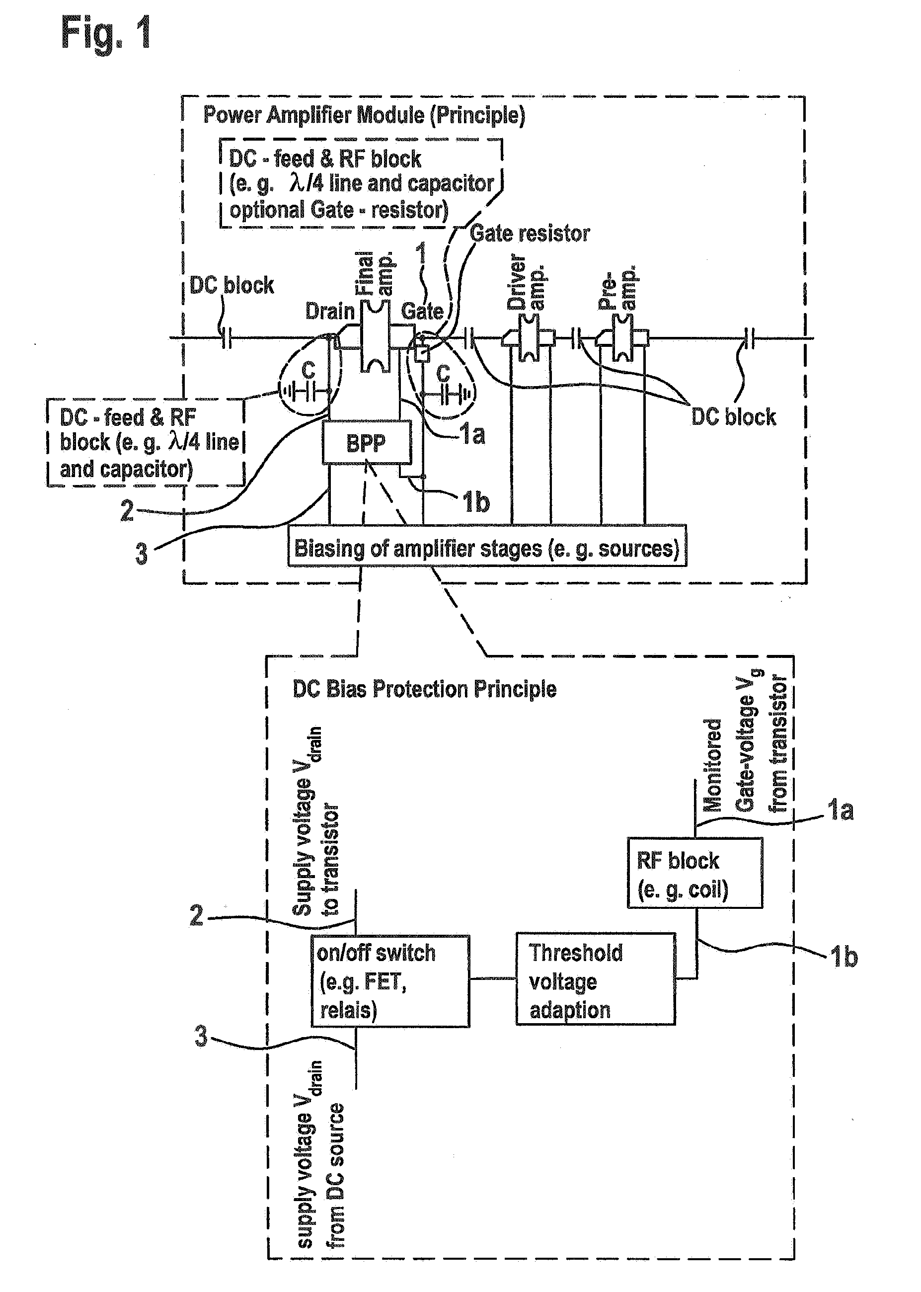
[0020]In FIG. 1 is shown a power amplifier module comprising in serial a preamplifier, a driver amplifier, a final amplifier and connected in parallel to their respective input and output a biasing of amplifier stages. It is the final amplifier which is made out of a depletion mode transistor according to the invention in the case shown in FIG. 1. But such a choice is not restrictive and it is by all means possible that it is the preamplifier and / or the driver amplifier which are made out of a depletion mode transistor according to the invention.

[0021]In the enlarged view of the FIG. 1 is shown the DC-bias protection principle of the depletion mode transistor according to the invention. A threshold voltage adaptation is connected to the Gate (1) of the depletion mode transistor. Two tapping-alternatives for Gate-voltage monitoring are possible:[0022]a) The input of the threshold voltage adaptation is directly connected to the Gate RF matching network via a RF block (position 1a). Th...


PUM


Abstract

A power amplifier bias protection for a depletion mode transistor is achieved according to the invention with a threshold voltage adaptation connected to the Gate of the depletion mode transistor. That threshold voltage adaptation controls a supply voltage switch for the Drain of the depletion mode transistor such that when the threshold voltage adaptation measures a voltage applied to that Gate outside a tolerable predefined range, then it activates the supply voltage switch to disconnect the Drain DC feed line. The input of the supply voltage switch is connected to the Drain voltage source of the depletion mode transistor and the output of the supply voltage switch is connected to the Drain DC feed line.

Description

TECHNICAL FIELD[0001]The present invention relates to an amplifier with a depletion mode transistor. Furthermore, the present invention is related to a method for controlling the Gate-voltage to be applied to a depletion mode transistor from an amplifier. The invention concerns also a terminal for radio telecommunications like a broadband, multi-band or wideband base station or a telecommunications terminal (mobile phone) supporting single- or multi-standard operation.BACKGROUND OF THE INVENTION[0002]The invention is based on a priority application EP 06290176.4 which is hereby incorporated by reference.[0003]To cover different frequency bands and mobile communication standards by a single base station, highly linear and efficient multiband / multistandard capable amplifier modules are required. The problem lies with current silicon-based Laterally Diffused Metal Oxide Silicon LDMOS RF power transistors—which often form the basis of power amplifiers. By use of LDMOS-based power amplif...

Claims


Application Information

Patent Timeline
Patent Type & Authority Applications(United States)
IPC IPC(8): H03G3/20
CPCH03F1/30H03F1/52H03F1/523H03F2200/507H03F2200/15H03F2200/471H03F3/189
Inventor SEYFRIED, ULRICHWIEGNER, DIRK
Owner ALCATEL LUCENT SAS
Why Eureka
Try Eureka