Method and apparatus to provide compensation for parasitic inductance of multiple capacitors
- Summary
- Abstract
- Description
- Claims
- Application Information
AI Technical Summary
Benefits of technology
Problems solved by technology
Method used
Image
Examples
example
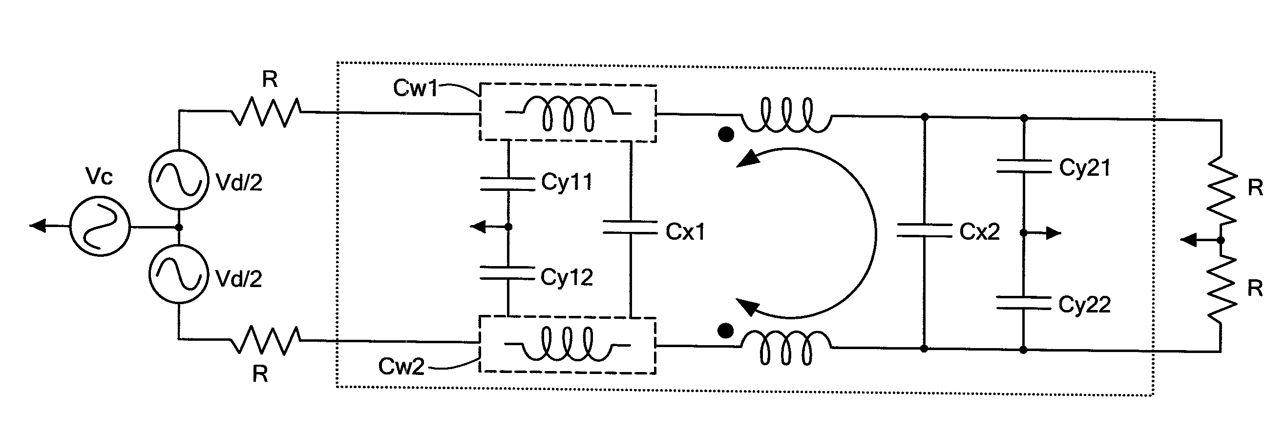
[0064] A commercially available filter was used as a starting point as shown in FIG. 15A, which shows a filter schematic, and FIG. 15B, which shows a pictorial representation of the filter. As can be seen in FIG. 15B, the relatively large (15 μH) series inductors L11 and L12 are particularly bulky, heavy, and expensive components of the commercial filter. Thus, it would be desirable to eliminate them while preserving filter performance. In the illustrated filter, exemplary component values are set forth below in Table 1:
TABLE 1Impedance ValuesComponentValueL11, L12 15 μHCY11, CY12 47 nF film capacitorCX1, CX22.2 μF film capacitorCY21, CY22 15 nF ceramic capacitor
[0065] As shown in FIGS. 16A (schematic) and 16B (pictorial representation), the series inductors (L11, L12 of FIG. 15B) were thus removed to provide working space for installing inductance cancellation windings CW1, CW2. Removal of the series inductors is offset through use of the significantly smaller cancellation windin...
PUM
 Abstract
Description
Claims
Application Information


