Nonvolatile semiconductor memory device

Active Publication Date: 2005-07-12
MONTEREY RES LLC
View PDF6 Cites 29 Cited by
  • Summary
  • Abstract
  • Description
  • Claims
  • Application Information

AI Technical Summary

Benefits of technology

[0028]Because the first global digit line and the second global digit line are disposed adjacent each other, noise applied to a global digit line is transmitted to the other global digit line, so that there is equivalent noise between the first and second global digit lines. That is, noise of the same phase is applied between the first and second global digit lines. By disposing the first and second global digit lines adjacent each other, effects of the noise can be canceled by each other in the reading operation with both the global digit lines as a pair.
[0029]Because the reference side has the same path configuration as the cell information propagating path on the cell information side and the both paths are dispo

Problems solved by technology

Therefore, parasitic capacitance between input signal lines on memory cell information side and reference side in each differential amplifier 106 is unbalanced.
The diameter of the wafer has been increased at the same time, and thus there is a fear that the difference in the wafer face may also increase.
Thus, even if the capacitance loads CLD1, CLD2 including the characteristics of both the parasitic element components are applied at the design stage, it is difficult to match the characteristic of the reference side with the characteristic of the parasitic element component, including these variable factors, because

Method used


Image

  • Nonvolatile semiconductor memory device
  • Nonvolatile semiconductor memory device
  • Nonvolatile semiconductor memory device

Examples


Example

[0067]Hereinafter, the first through fourth embodiments of the nonvolatile semiconductor memory device of the present invention will be described in detail with reference to FIGS. 1 through 21.

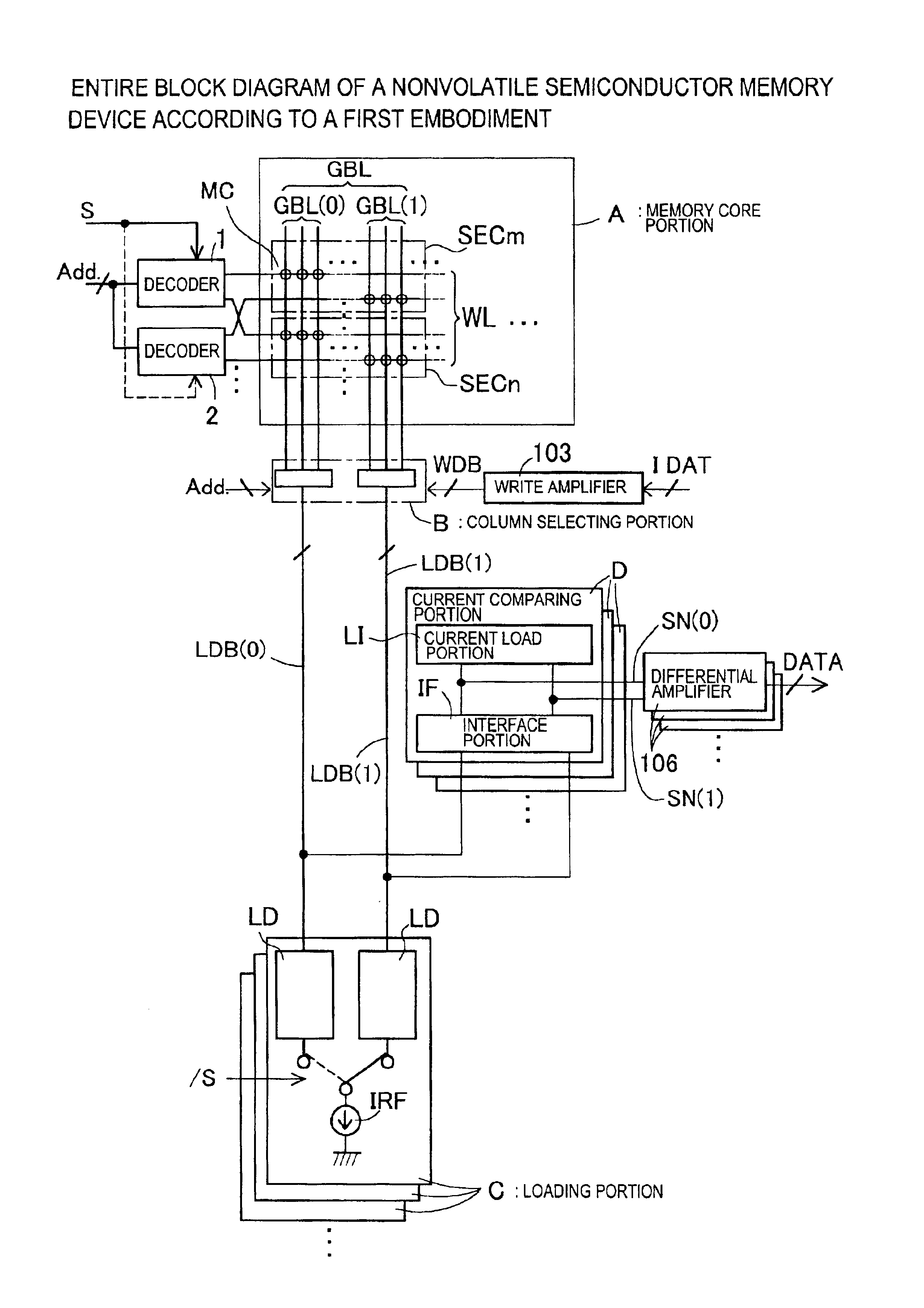
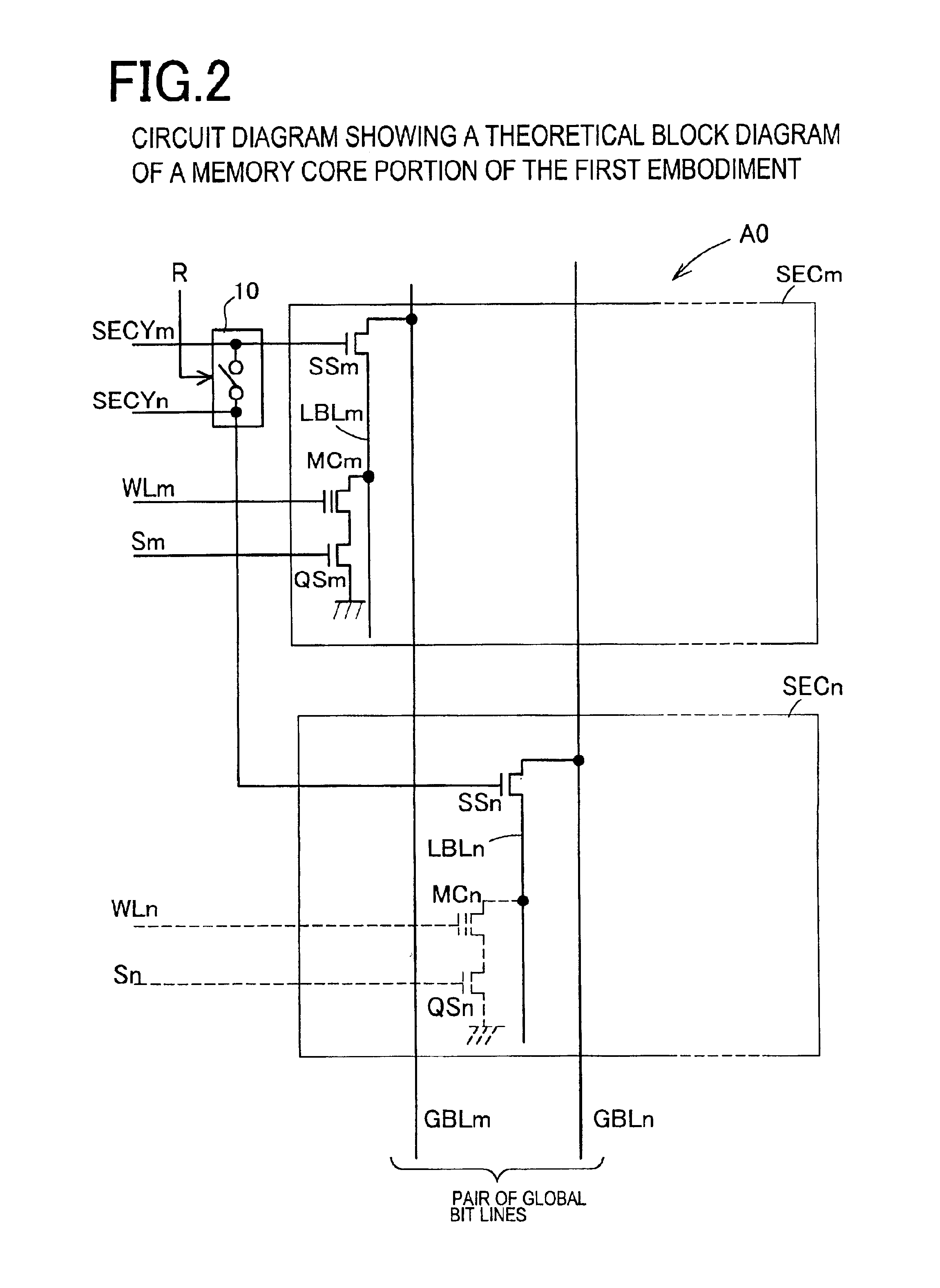
[0068]First, FIG. 1 shows an entire structure of the nonvolatile semiconductor memory device of the first embodiment. Referring to the entire block diagram of FIG. 1, a memory core portion A and a column selecting portion B are provided instead of the memory core portion A100 and the column selecting portion B100 in a conventional nonvolatile semiconductor memory device shown in FIG. 22. Because the selecting method of the global bit line GBL in the memory core portion A is different from the memory core portion A100, as the word line WL selecting decoder, decoders 1, 2 are provided instead of the decoder 101. Further, instead of the reference bus line RB dedicated for reference and the data bus line LDB commonly used for reading and programming, as data bus line for reading, data bus lines LD...

Example

[0130]According to the first embodiment shown in FIG. 1 and second to fourth embodiments to be described later, by combining concrete examples of the memory core portion A, column selecting portion B, loading portion C and current comparing portion D described above, appropriately, the nonvolatile semiconductor memory device of the present invention can be constructed.

[0131]The present invention is not restricted to the first embodiment, and, needless to say, may be improved or modified within a scope not departing from the purpose of the present invention.

[0132]For example, although a case in which the local bit lines LBLm, LBLn connected to a pair of the global bit lines GBLm, GBLn (FIG. 2) are disposed in adjacent sectors SECm, SECn has been described in the first embodiment, the present invention to is not restricted to this example, but the local bit lines may be disposed adjacent each other. In a memory core portion A20 according to a second embodiment shown in FIG. 19, as sho...


PUM


Abstract

This invention provides a nonvolatile semiconductor memory device including a novel memory core portion in which an influence of a parasitic element component in a memory cell information reading path is excluded in a reading operation, and novel sensing means accompanying this memory core structure, so as to achieve rapid sensing. In the memory core portion, a selected memory cell is selected by a global bit line through a local bit line and an adjacent global bit line is connected to a local bit line in a non-selected sector. A column selecting portion connects a pair of the global bit lines to a pair of data bus lines. A load portion having a load equivalent to a parasitic capacitance of a path leading from the memory cell and for supplying a reference current to a reference side is connected to a pair of the data bus lines. A current of the memory cell information is compared with the reference current by a current comparing portion and a differential current is outputted. A path load is equalized by a pair of adjacent paths so that an effect from noise is canceled, thus making it possible to achieve rapid reading.

Description

BACKGROUND OF THE INVENTION[0001]1. Field of the Invention[0002]The present invention relates to an operation for reading memory cell information in a nonvolatile semiconductor memory device, and more particularly to high-speed sensing technology for the reading operation.[0003]2. Description of the Related Art[0004]In a nonvolatile semiconductor memory device such as a flash memory, storage of memory cell information is carried out by current driving power of a nonvolatile transistor in the nonvolatile memory cell. That is, the storage of the memory cell information is carried out according to a difference such as whether or not the nonvolatile transistor allows a current to flow with respect to memory cell information of “1” / “0” or whether it supplies a larger amount of current or a smaller amount of current.[0005]Then, sensing of the memory cell information stored in the nonvolatile semiconductor memory device is carried out depending on whether or not a current flows through a d...

Claims


Application Information

Patent Timeline
IPC IPC(8): G11C7/18G11C7/00G11C16/28G11C16/06G11C16/04G11C16/24
CPCG11C7/18G11C16/24G11C16/28G11C16/06
Inventor SHIMBAYASHI, KOJIFURUYAMA, TAKAAKI
Owner MONTEREY RES LLC
Why Eureka
Try Eureka