Solid-state imaging device and camera

a solid-state imaging and camera technology, applied in the field of solid-state imaging devices and cameras, can solve the problems of sensitivity degradation, difficulty in thinning a breadth of light shielding walls b>606, etc., and achieve the effect of high image quality

Inactive Publication Date: 2007-08-16
PANASONIC CORP
View PDF13 Cites 44 Cited by
  • Summary
  • Abstract
  • Description
  • Claims
  • Application Information

AI Technical Summary

Benefits of technology

[0021]A camera according to the present invention is a camera having a solid-state imaging device, the solid-state imaging device comprising: two-dimensionally arrayed pixels; a plurality of color filters each operable to transmit light of a wavelength predetermined for each pixel; and a light shielding wall operable to partition the color filters for ea...

Problems solved by technology

On the other hand, it is difficult to thin a breadth of the light shielding wall 606 made from the resin material that partitions the co...

Method used


Image

  • Solid-state imaging device and camera
  • Solid-state imaging device and camera
  • Solid-state imaging device and camera

Examples


Embodiment Construction

[0030]The following describes an embodiment of a solid-state imaging device and a camera according to the present invention using a digital camera as an example, with reference to the drawings.

[1] Structure of Digital Camera

[0031]First, a structure of a digital camera according to an embodiment is described.

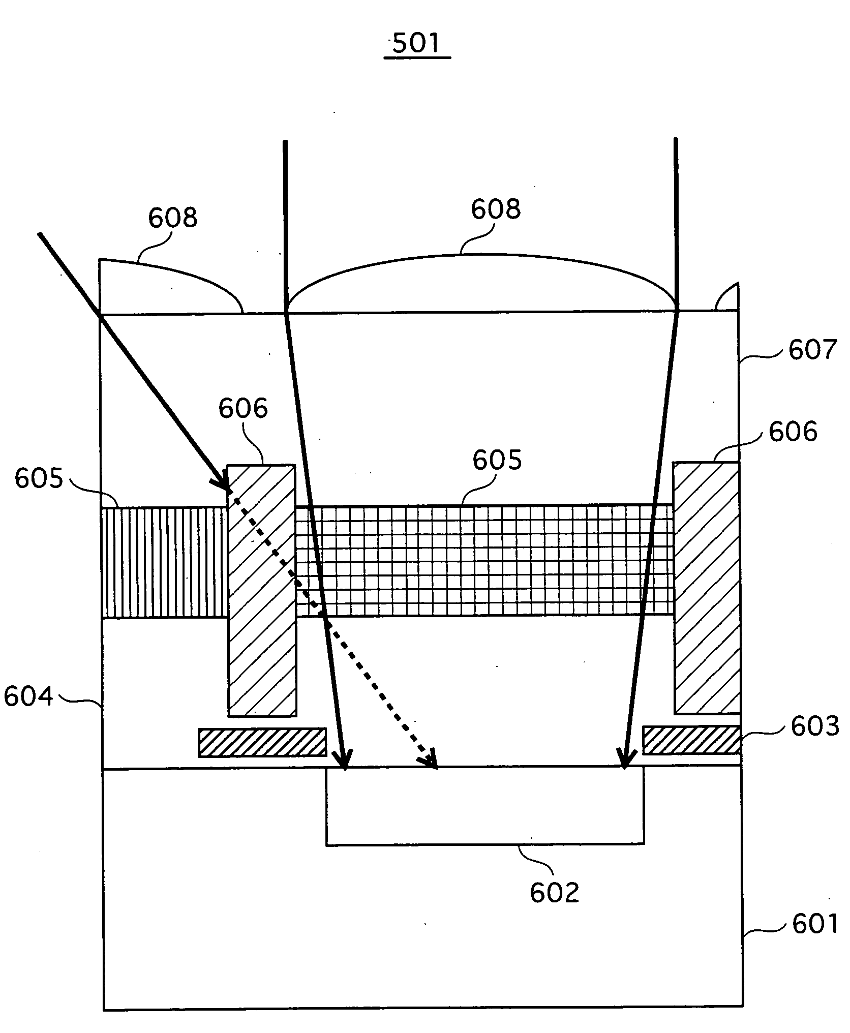
[0032]FIG. 3 is a sectional view showing a structure of the digital camera according to the embodiment. As shown in FIG. 3, a digital camera 1 includes a solid-state imaging device 101, an imaging lens 102, a cover glass 103, a gear 104, an optical finder 105, a zoom motor 106, a finder eyepiece 107, an LCD (liquid crystal display) monitor 108, and a circuit board 109.

[0033]A user of the digital camera 1 observes a subject by looking through the optical finder 105 through the finder eyepiece 107 to select a camera angle. Also, the user operates the zoom motor 106 to adjust a zoom of the imaging lens 102 via the gear 104.

[0034]Light from the subject transmits the cover glass 103 a...


PUM


Abstract

A solid-state imaging device 101 is composed of a transparent film 204, a color filter 205, a planarizing film 207, and a plurality of microlenses 208 that are sequentially formed on a semiconductor substrate 201. A photodiode 202 is formed in a surface of the semiconductor substrate 201 that is closer to the transparent film 204. A light shielding film 203 is formed in a surface of the transparent film 204 that is closer to the semiconductor substrate 201. Color filters 205 respectively corresponding to two adjacent pixels are partitioned by a light shielding wall 206. The light shielding wall 206 is a λ/4 multilayer film that reflects visible light.

Description

CROSS-REFERENCE TO RELATED APPLICATIONS[0001]This application is based on application No. 2006-038598 filed in Japan, the contents of which are hereby incorporated by reference.BACKGROUND OF THE INVENTION[0002](1) Field of the Invention[0003]The present invention relates to a solid-state imaging device and a camera, and particularly to a light shielding technique for preventing light that transmits a color filter from entering an unintended photoelectric device.[0004](2) Related Art[0005]Solid-state imaging devices that have spread widely in recent years image in color by detecting light intensity of each color using color filters.[0006]FIG. 1 is a block diagram showing a structure of a solid-state imaging device according to a conventional art. As shown in FIG. 1, a solid-state imaging device 5 includes a plurality of pixels 501, a vertical shift register 502, a vertical signal line 503, a column memory 504, a horizontal shift register 505, a horizontal signal line 506, and an outp...

Claims


Application Information

Patent Timeline
IPC IPC(8): H04N9/04
CPCH01L27/14621H01L27/14643H01L27/14627H01L27/14623
Inventor YAMAGUCHI, TAKUMIINABA, YUICHIUEDA, DAISUKE
Owner PANASONIC CORP
Why Eureka
Try Eureka