Enhanced delay matching buffer circuit

a delay matching and buffer circuit technology, applied in the field of buffer circuits, can solve the problems of difficult correlation between the io circuitry and the core logic circuitry, difficulty in achieving good matching over process, and difficulty in achieving supply voltage and temperature variations to which the chip may be subjected, and achieve the effect of improving the matching delay

Active Publication Date: 2007-08-23
AVAGO TECH INT SALES PTE LTD
View PDF8 Cites 11 Cited by
  • Summary
  • Abstract
  • Description
  • Claims
  • Application Information

AI Technical Summary

Benefits of technology

[0006] The present invention meets the above-noted need by providing, in an illustrative embodiment thereof, a buffer circuit architecture suitabl

Problems solved by technology

In applications where an internal matching buffer is required to match the delay of an input buffer that brings an external signal inside of a semiconductor chip, achieving good matching over process, supply voltage, and temperature (PVT) variations to which the chip may be subjected is often difficult.
Because of the different supply voltages at which the two types of transistors operate and the different process parameters associated with the two types of transistors, correlation between the

Method used


Image

  • Enhanced delay matching buffer circuit
  • Enhanced delay matching buffer circuit
  • Enhanced delay matching buffer circuit

Examples


Embodiment Construction

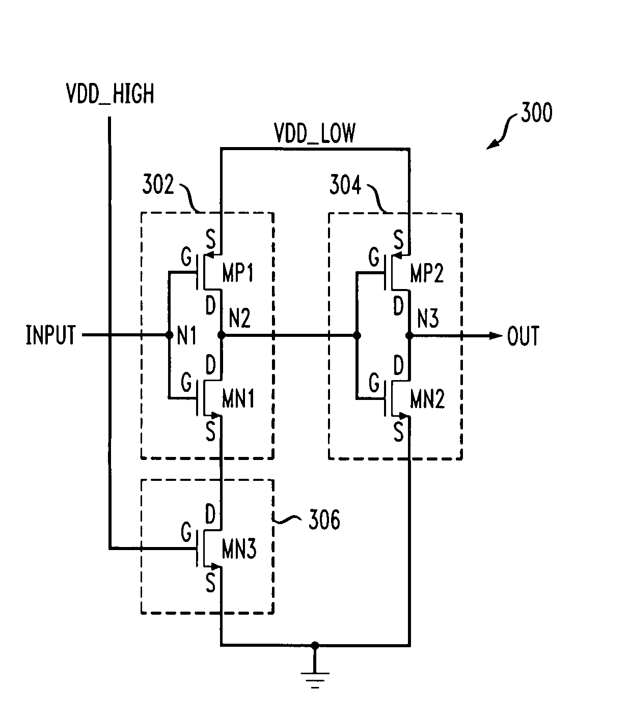
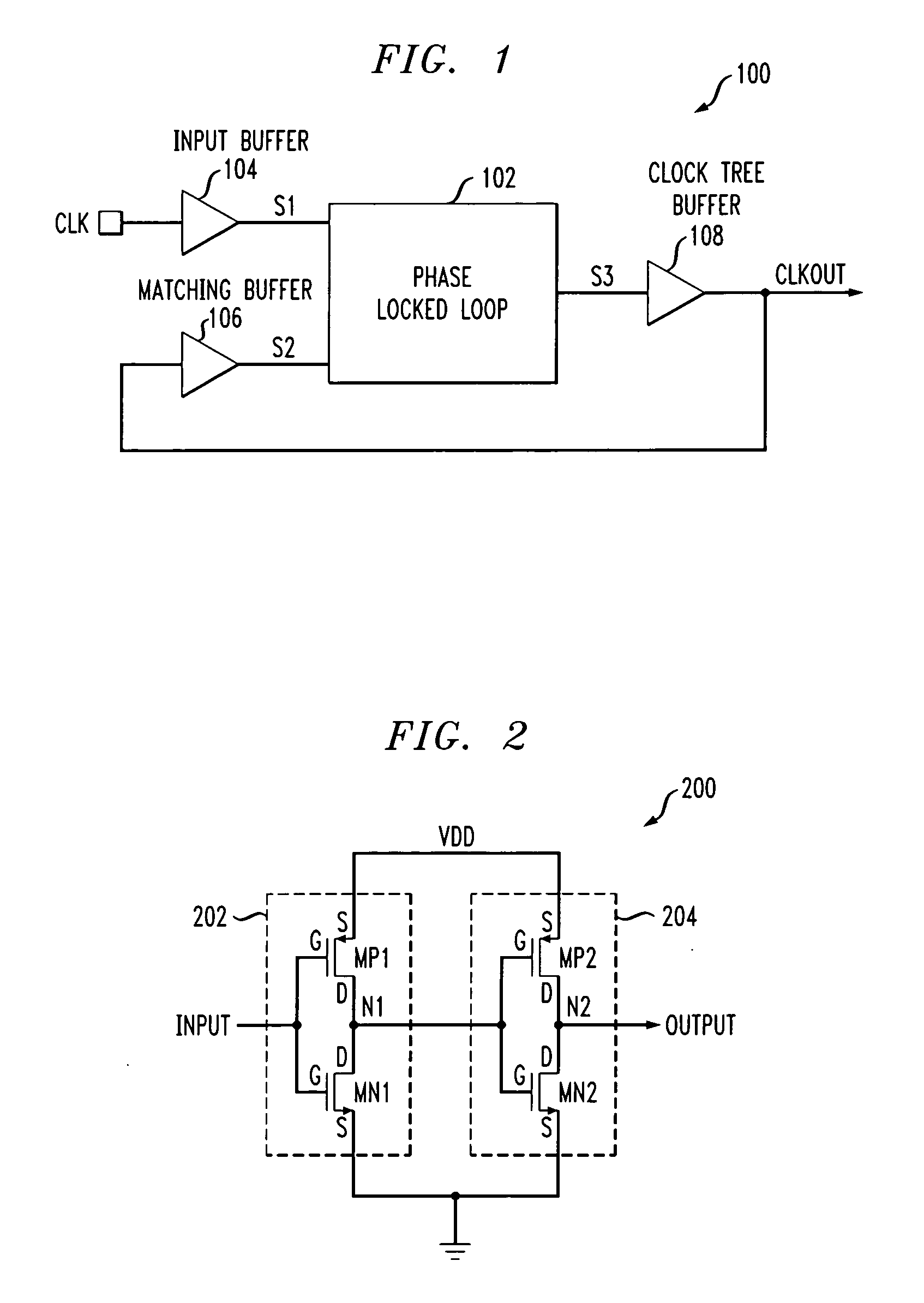
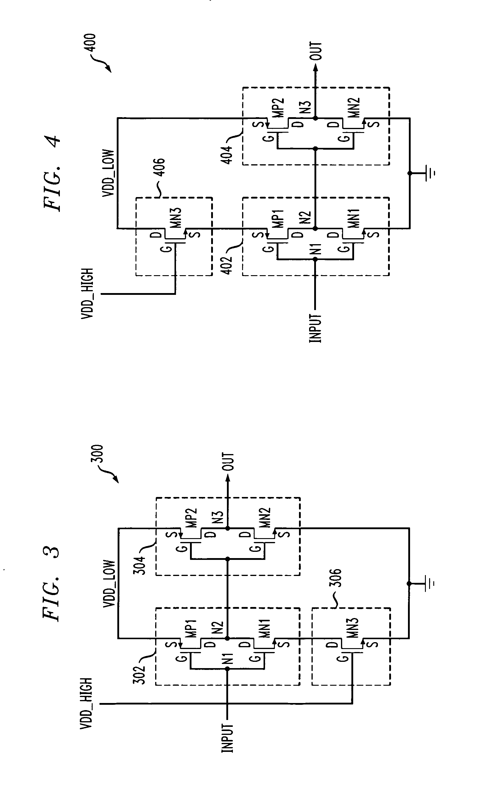
[0015] The present invention will be described herein in the context of illustrative matching buffer circuits for use, for example, in a PLL circuit. It should be understood, however, that the present invention is not limited to this or any other particular buffer circuit and / or application. Rather, the invention is more generally applicable to an improved buffer circuit for providing enhanced delay matching between the buffer circuit and a second buffer adapted to interface with external signals. Moreover, the techniques of the present invention essentially eliminate the need for additional delay matching circuitry and / or the need for increasing a timing budget of the circuit in which the buffer circuit is employed. Although implementations of the present invention are described herein with specific reference to p-channel metal-oxide-semiconductor (PMOS) and n-channel metal-oxide-semiconductor (NMOS) transistor devices, as may be formed using a complementary metal-oxide-semiconduct...


PUM


Abstract

A buffer circuit includes an input stage including at least one MOS device having a first threshold voltage associated therewith, the input stage being adapted to receive an input signal referenced to a first voltage supply. The buffer circuit further includes an output stage including at least one MOS transistor having the first threshold voltage associated therewith, an input of the output stage being connected to an output of the input stage, the output stage being operative to generate an output signal which is indicative of a logic state of the input signal. The buffer circuit includes a delay control circuit adapted for connection between at least one of the first voltage supply and a voltage return of the buffer circuit, and at least one of the input stage and the output stage. The delay control circuit includes at least one MOS device having a second threshold voltage associated therewith. The MOS device in the delay control circuit being adapted to receive, as a control signal, a second voltage supply, a delay of the buffer circuit being at least partially controlled as a function of a process parameter, the second voltage supply and/or a temperature of the MOS device in the delay control circuit.

Description

FIELD OF THE INVENTION [0001] The present invention relates generally to electronic circuits, and more particularly relates to buffer circuits. BACKGROUND OF THE INVENTION [0002] Many electronic devices employ buffers to interface with external signals. These buffers have certain respective delays associated therewith. In applications where an internal matching buffer is required to match the delay of an input buffer that brings an external signal inside of a semiconductor chip, achieving good matching over process, supply voltage, and temperature (PVT) variations to which the chip may be subjected is often difficult. One exemplary application in which it is desirable to use an internal matching buffer is for phase alignment in a phase-locked loop (PLL) circuit, where the chip level design requires the removal of clock tree build-up delay and / or removal of the delay of the reference clock input buffer delay. [0003] In many earlier technologies, core logic circuitry typically operate...

Claims


Application Information

Patent Timeline
IPC IPC(8): H03B1/00
CPCH03K19/00323H03K5/133H03K19/00384
Inventor NELSON, DALE
Owner AVAGO TECH INT SALES PTE LTD
Why Eureka
Try Eureka