

LED assembly and manufacturing method
a technology of led assemblies and manufacturing methods, applied in the direction of electrical equipment, coupling device connections, semiconductor devices, etc., can solve the problems of low heat dissipation performance of the above structure and troublesome electrostatic breakdown, and achieve good antistatic characteristics and efficient heat dissipation
- Summary
- Abstract
- Description
- Claims
- Application Information
AI Technical Summary
Benefits of technology
Problems solved by technology
Method used
Image

Examples
first exemplary embodiment
[0052] An LED assembly and its manufacturing method in the first exemplary embodiment of the present invention are described below with reference to drawings.
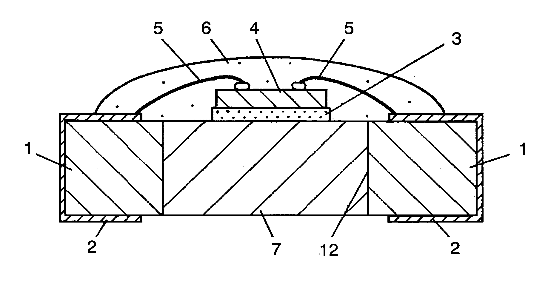
[0053]FIG. 1 is a sectional view illustrating the structure of a surface-mount LED assembly in the first exemplary embodiment of the present invention. FIG. 2 is a sectional view of another example of the LED assembly.
[0054] In FIG. 1, wiring substrate 1 is preferably a resin substrate, typically made of glass-epoxy resin, or a ceramic substrate, typically an alumina substrate. Wiring pattern 2, which acts as both wiring and a terminal electrode of a surface-mount assembly, is formed on this wiring substrate 1. This wiring pattern 2 is preferably made of an electrode material, typically copper or silver.
[0055] Opening 12 is created at the center of this wiring substrate 1. Heat sink 7, which has better heat conductivity than wiring substrate 1, is disposed inside this opening 12. LED chip 4 is die-bonded onto one face of thi...
second exemplary embodiment
[0081] An LED assembly and its manufacturing method in the second exemplary embodiment of the present invention are described below with reference to drawings.
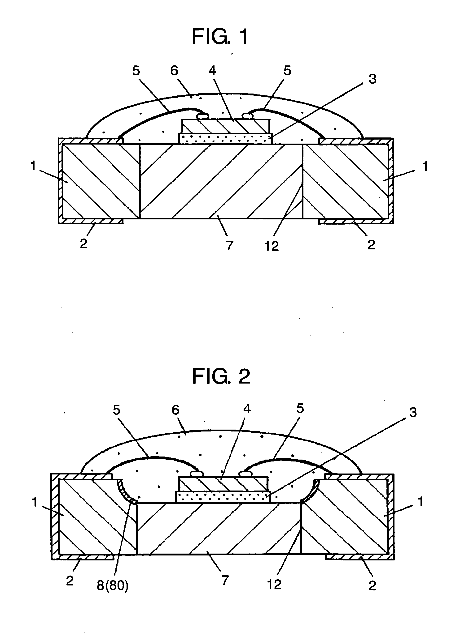
[0082]FIG. 8 is a sectional view illustrating the structure of a surface-mount LED assembly in the second exemplary embodiment of the present invention. FIG. 9 is a sectional view of another example.
[0083] In FIGS. 8 and 9, a significant difference in the structure of the LED assembly in the second exemplary embodiment, compared to that of the first exemplary embodiment, is the shape of heat sinks 7a and 7b. Heat sinks 7a and 7b in the second exemplary embodiment are characterized by their cavity created by making a concave portion.
[0084] Heat sinks 7a and 7b shown in FIGS. 8 and 9 have a cavity formed by machining metal with good heat conductivity, typically aluminum, copper, or silver. A space for mounting LED chip 4 is provided on the bottom of this cavity.
[0085] The inner periphery of the concave portion which forms th...
third exemplary embodiment
[0092] An LED assembly and its manufacturing method in the third exemplary embodiment of the present invention are described below with reference to drawings.
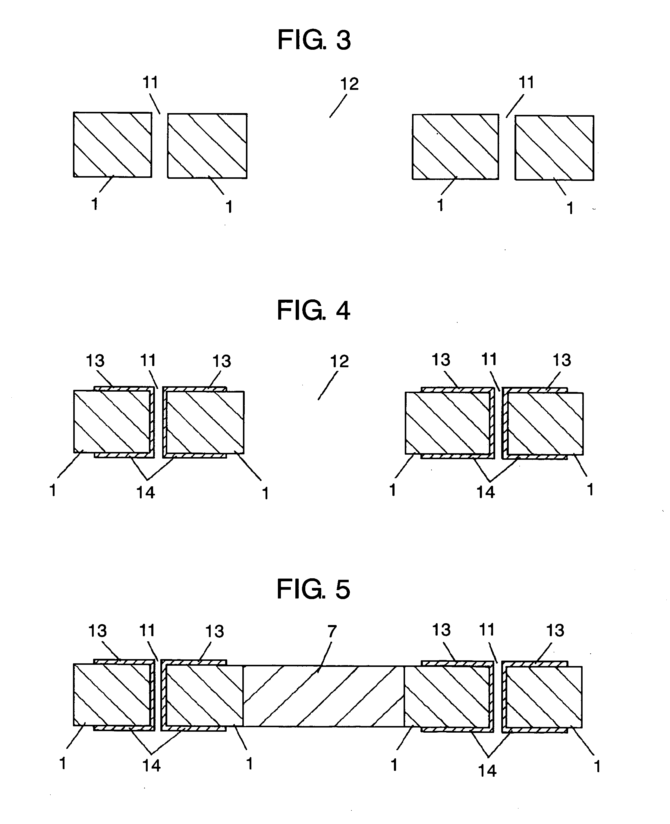
[0093] FIGS. 10 to 13 are sectional views illustrating the manufacturing method of LED assembly in the third exemplary embodiment of the present invention. FIG. 14 is a sectional view of another example of the LED assembly.
[0094] A surface-mount LED assembly in the third exemplary embodiment of the present invention basically has a structure shown in FIG. 8. A significant difference in the LED assembly in the third exemplary embodiment, compared to that of the second exemplary embodiment, is the material of heat sink 7a. The LED assembly in the third exemplary embodiment uses heat sink 7c instead of heat sink 7a in FIG. 8. This heat sink 7c is made of resin containing metal filler (heat-conducting filler) which has good heat conductivity. This metal filler used for heat sink 7c is described next. First, resin paste is made by...
PUM
 Abstract
Description
Claims
Application Information