Device For Detecting Defects Which Are Deep And Close To The Surface In Electrically Conductive Materials In A Nondestructive Manner

a technology of electrically conductive materials and devices, applied in the direction of magnetic properties, instruments, material magnetic variables, etc., can solve the problems of physical impeded by skin effect, poor spatial resolution, limited fault size,

Inactive Publication Date: 2007-08-30
SIEMENS AG
View PDF12 Cites 11 Cited by
  • Summary
  • Abstract
  • Description
  • Claims
  • Application Information

AI Technical Summary

Benefits of technology

[0006] The invention is therefore based on the object of developing a device of the type mentioned at the outset such that it can advantageously be used over a relatively wide frequency range and therefore, firstly, can detect deep, hidden faults and surface faults and, secondly, a quantitative relationship is made possible between the detector signal and the defect size and depth and such that, finally, the quality of the sensor can be fully utilized even in an environment with electromagnetic interference.

Problems solved by technology

In order to obtain information, by means of an eddy-current method, from the deep material regions, i.e. from depths of greater than 1 mm, it is necessary to produce very strong eddy-current fields at the depth of the component, which is physically impeded by the skin effect, however.
Low frequencies penetrate very deep into the material, but have, purely physically, a poor spatial resolution, and therefore the fault size which can be detected is limited.
Higher frequencies have a better spatial resolution but, as the frequency increases, the measurement sensitivity is restricted to an ever greater extent by electromagnetic interference effects.

Method used


Image

  • Device For Detecting Defects Which Are Deep And Close To The Surface In Electrically Conductive Materials In A Nondestructive Manner
  • Device For Detecting Defects Which Are Deep And Close To The Surface In Electrically Conductive Materials In A Nondestructive Manner
  • Device For Detecting Defects Which Are Deep And Close To The Surface In Electrically Conductive Materials In A Nondestructive Manner

Examples


Embodiment Construction

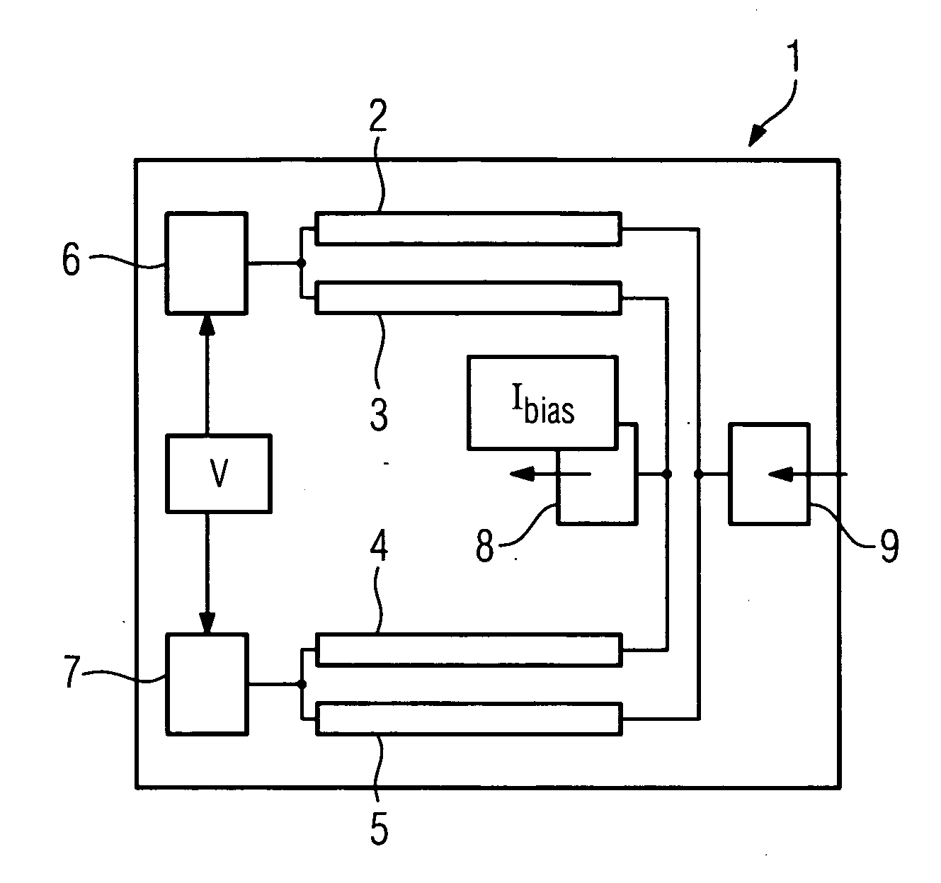
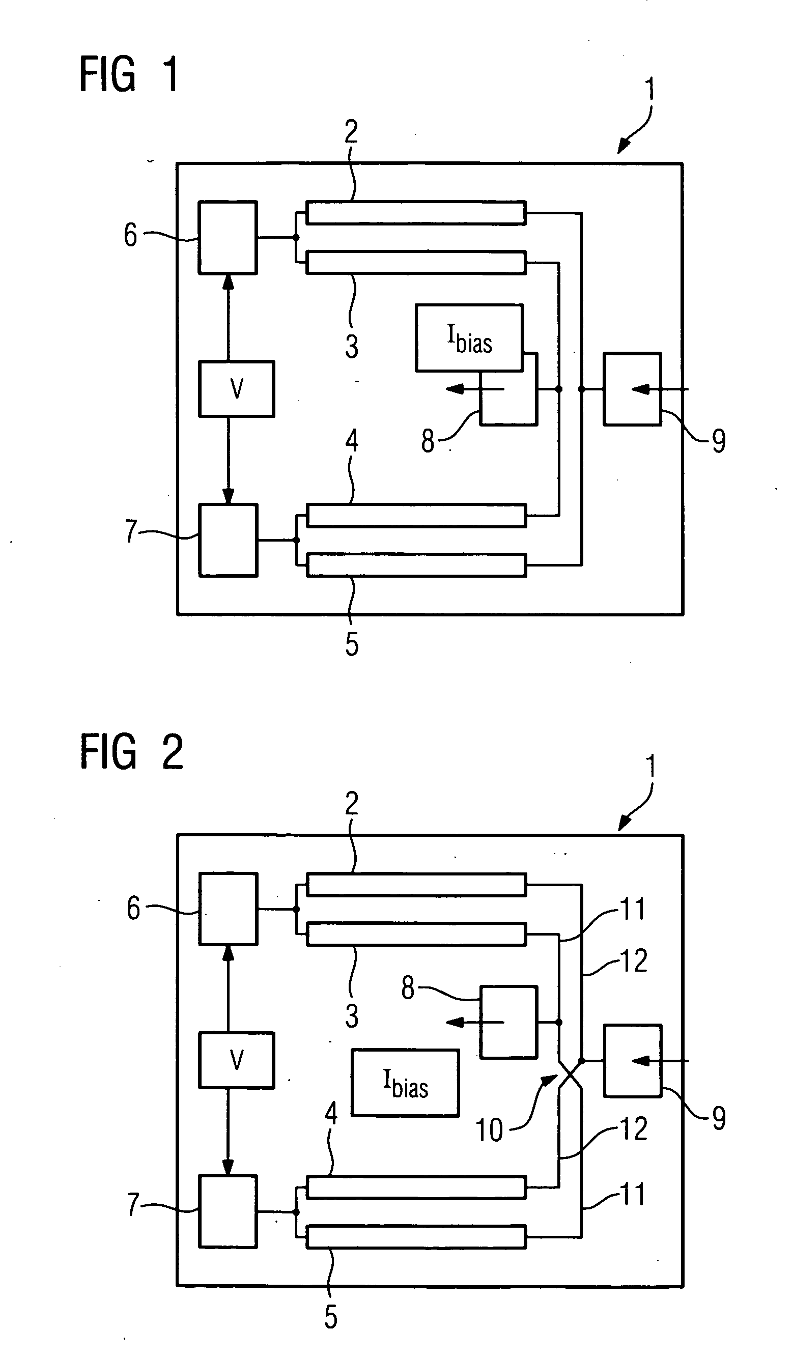
[0020]FIG. 1 shows a chip 1, on which an integrated bridge circuit comprising four magnetically sensitive resistors 2 to 5 is arranged, 6 and 7 indicating contact areas for connecting the tap-off lines for the resulting measured voltage V, and 8 and 9 indicating corresponding conductor connections for feeding a supply current Ibias into the converter bridge.

[0021] The bridge circuit with the chip feed lines (13, 14, 15, 16) is designed to have such a low inductance that the signal output voltage of the bridge circuit is essentially proportional to the magnetic field of the eddy currents and not their induction.

[0022] In the arrangement shown in FIG. 2, the loop area is also folded (see point of intersection 10 between the connecting lines 11 and 12, which in this case are of course guided one over the other in isolated fashion).

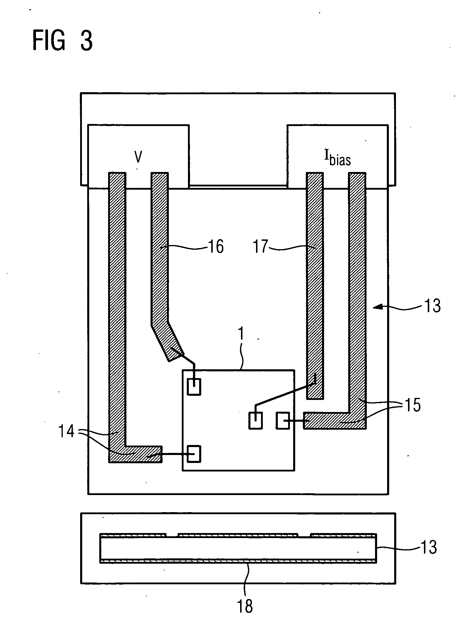
[0023] Such a low-induction converter bridge as shown in FIGS. 1 and 2 is integrated in an eddy-current measuring head so as to avoid substantial inductiv...


PUM

PropertyMeasurementUnit
depthsaaaaaaaaaa
frequencyaaaaaaaaaa
electrically conductiveaaaaaaaaaa

Abstract

The invention relates to a device for detecting defects which are deep in electrically conductive materials in a non-destructive manner, comprising an excitation device provided with induction coils which are used to produce low frequency eddy currents in the material, and a receiving device for the magnetic field of the eddy currents, said magnetic field being modified by the defects, and said receiving device comprising a gradiometer magnetic field sensors with an integrated bridge circuit.

Description

CROSS REFERENCE TO RELATED APPLICATIONS [0001] This application is the US National Stage of International Application No. PCT / EP2005 / 001888, filed Feb. 23, 2005 and claims the benefit thereof. The International Application claims the benefits of European Patent application No. 04005462.9 filed Mar. 8, 2004. All of the applications are incorporated by reference herein in their entirety.FIELD OF THE INVENTION [0002] The invention relates to a device for detecting defects which are deep and close to the surface in electrically conductive materials in a nondestructive manner, having an exciter device with induction coils for producing low-frequency eddy currents in the material, and having a reception device for the magnetic fields of the eddy currents, which fields have been changed by the defects. BACKGROUND OF THE INVENTION [0003] The conventional solution to the problem of detecting deep defects in electrically conductive materials in a nondestructive manner is the use of a low-freq...

Claims


Application Information

Patent Timeline
Patent Type & Authority Applications(United States)
IPC IPC(8): G01N27/82G01N27/90
CPCG01N27/9033G01N27/9006
Inventor DAALMANS, GABRIELSTECK, MARTIN
Owner SIEMENS AG
Why Eureka
Try Eureka