Manufacturing method for a solid-state imaging apparatus, and the solid-state imaging apparatus

a solid-state imaging and manufacturing method technology, applied in the direction of television systems, radiation controlled devices, color signal processing circuits, etc., can solve the problems of poor contact between the electrodes and the wires, the inability to reduce the parasite capacity of the floating diffusion region, and the inability to improve the sensitivity of the solid-state imaging apparatus. achieve the effect of effectively preventing

Inactive Publication Date: 2007-08-30
PANASONIC CORP
View PDF4 Cites 26 Cited by
  • Summary
  • Abstract
  • Description
  • Claims
  • Application Information

AI Technical Summary

Benefits of technology

[0052] According to the stated structure, the translucent adhesive ca

Problems solved by technology

However, merely combining the structures taught by the aforementioned patent documents gives rise to a problem that when attaching the translucent plate to the semiconductor substrate, the translucent adhesive (an organic material such as epoxy resin) flows into the area corresponding to the floating diffusion region on the semiconductor substrate, thus covering the floating diffusion region.
This means that the paras

Method used


Image

  • Manufacturing method for a solid-state imaging apparatus, and the solid-state imaging apparatus
  • Manufacturing method for a solid-state imaging apparatus, and the solid-state imaging apparatus
  • Manufacturing method for a solid-state imaging apparatus, and the solid-state imaging apparatus

Examples


first embodiment

[0084]

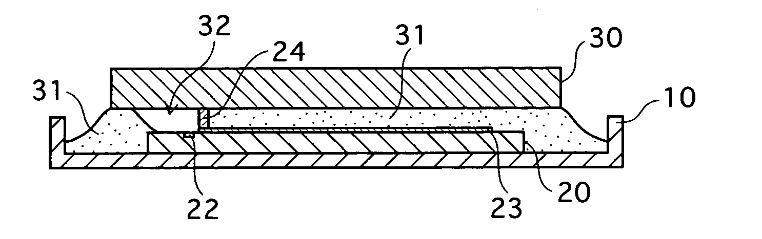
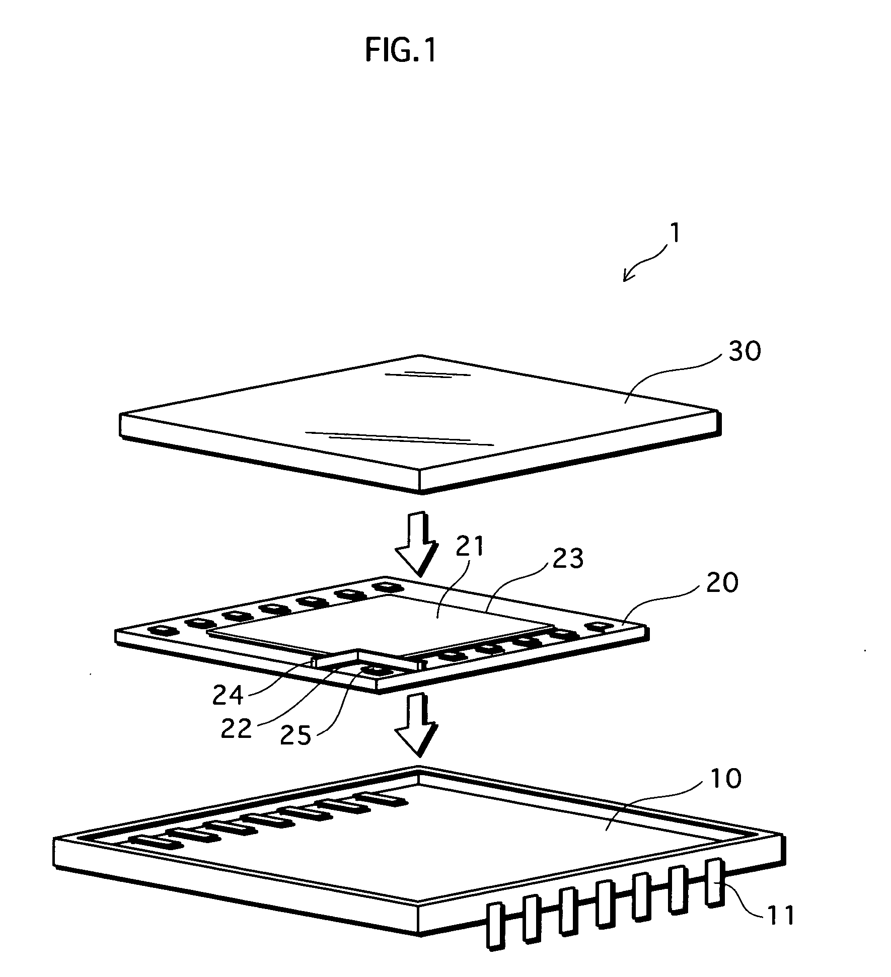
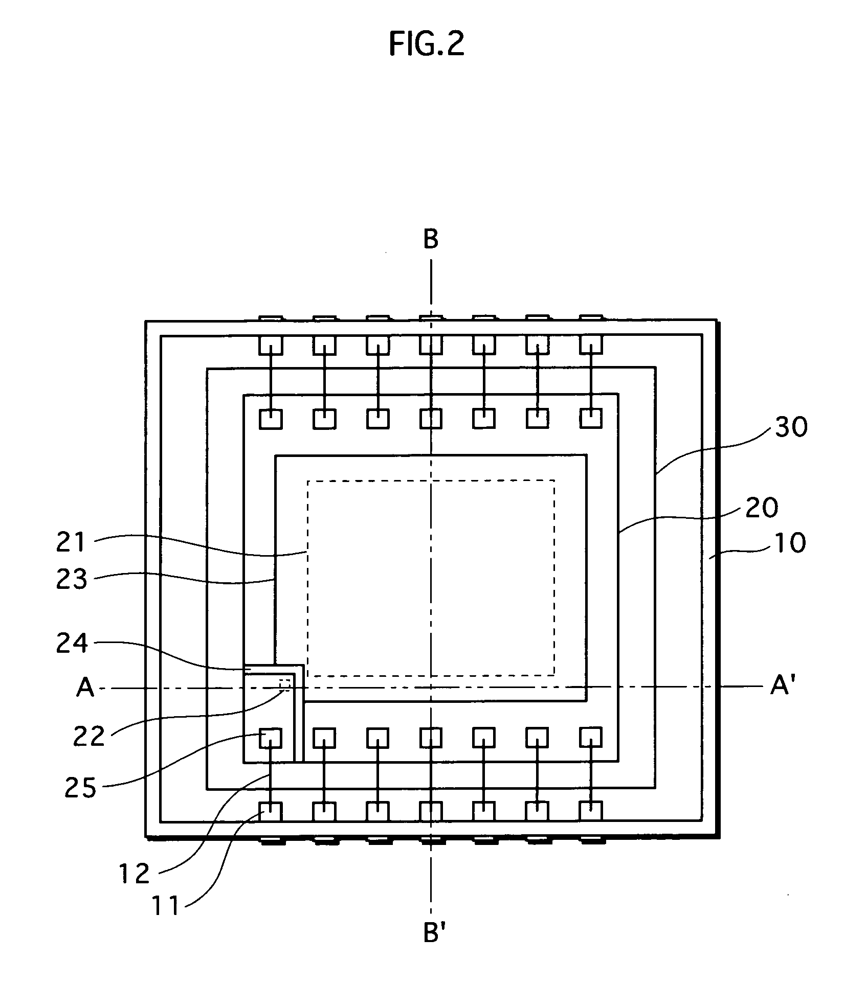
[0085]FIG. 1 is an exploded perspective view of a solid-state imaging apparatus 1 of the first embodiment, and FIG. 2 is a planar view of the solid-state imaging apparatus 1 of the first embodiment.

[0086] As shown in FIG. 1 and FIG. 2, the solid-state imaging apparatus 1 is composed of a package substrate 10, a semiconductor substrate 20, and a translucent plate 30. The package substrate 10 is made of a material such as ceramic or plastic, and has lead terminals 11. The semiconductor substrate 20 has a light receiving region 21 and a floating diffusion region 22 that is disposed apart from the light receiving region 21. The semiconductor substrate 20 is die-bonded to the package substrate 10. The translucent plate 30 is made of a non-organic material (e.g., borosilicate glass or silica glass), an organic material (e.g., acrylic resin or polycarbonate resin), or a hybrid of these materials, and is attached to the semiconductor substrate 20 by a translucent adhesive.

[0087] A d...

second embodiment

[0128]FIG. 11 shows a planar view of the solid-state imaging apparatus of the second embodiment.

[0129] In the second embodiment, the dam member 24 surrounds the area corresponding to the floating diffusion region 22 on the semiconductor substrate 20, and does not surround the electrodes 25 and the area corresponding to the light receiving region 21 on the semiconductor substrate 20. Furthermore, the package substrate 10 in the second embodiment is smaller than the package substrate 10 in the first embodiment.

[0130]FIGS. 12A and 12B are cross-sectional views of the solid-state imaging apparatus of the second embodiment.

[0131]FIG. 12A shows an E-E′ cross-section in the planar view of FIG. 11, and FIG. 12B shows an F-F′ cross-section in the planar view of FIG. 11.

[0132]FIG. 13 is an enlarged planar view of the semiconductor substrate 20 of the second embodiment.

[0133] In the second embodiment, the dam member 24 surrounds the area corresponding to the floating diffusion region 22 o...

third embodiment

[0136]FIG. 14 is a planar view of a solid-state imaging apparatus of the third embodiment.

[0137] In the third embodiment the dam member 24 surrounds the area corresponding to the floating diffusion region 22 on the semiconductor substrate 20, and does not surround the electrodes 25 and the area corresponding to the light receiving region 21 on the semiconductor substrate 20. The package substrate 10 in the third embodiment is smaller than the package substrate 10 in the first embodiment, and larger than the package substrate 10 in the second embodiment.

[0138]FIGS. 15A and 15B are cross-sectional views of the solid-state imaging apparatus of the third embodiment.

[0139]FIG. 15A shows a G-G′ cross-section in the planar view of FIG. 14, and FIG. 15B shows a H-H′ cross-section in the planar view of FIG. 14.

[0140]FIG. 16 is an enlarged planar view of the semiconductor substrate 20 of the third embodiment.

[0141] In the third embodiment, the dam member 24 surrounds the area correspondi...


PUM


Abstract

A light receiving region 21 and a floating diffusion region 22 are formed apart from each other in a semiconductor substrate 20 (S11), translucent adhesive 31 is applied to an area corresponding to the light receiving region 21 on the semiconductor substrate 20 (S22), and a translucent plate 30 is attached to the semiconductor substrate 20 on which the translucent adhesive 31 has been applied (S23). In this semiconductor manufacturing process, before the translucent adhesive 31 is applied, a dam member 24 is formed on the semiconductor substrate 20 so as to prevent the translucent adhesive 31 from flowing into an area corresponding to the floating diffusion region 22 on the semiconductor substrate 20 (S18).

Description

BACKGROUND OF THE INVENTION [0001] (1) Field of the Invention [0002] The present invention relates to a manufacturing method for a solid-state imaging apparatus used in digital cameras and the like, and the solid state imaging apparatus. [0003] (2) Description of the Related Art [0004] In the field of solid-state imaging apparatuses, research and development into techniques for improving sensitivity of solid-state imaging apparatuses are being widely carried out. Japanese Patent Application Publication No. H2-2675 discloses a technique for improving sensitivity by reducing the parasite capacity of a floating diffusion region. Generally in a solid-state imaging apparatus, a light receiving region and the floating diffusion region are formed apart from each other in the semiconductor substrate which is covered with an organic film to protect the surface. In Japanese Patent Application Publication No. H2-2675, the part of the organic film that covers the floating diffusion region is re...

Claims


Application Information

Patent Timeline
IPC IPC(8): H04N3/14H04N5/335H04N9/64H04N5/217
CPCH01L27/14618H01L27/14621H01L27/14627H01L27/14636H01L27/14683H01L27/14843H01L2224/49175H01L2924/01019H01L2224/32225H01L2224/48091H01L2224/73265H01L2224/83385H01L2924/00014H01L2224/05554H01L2924/16235H01L2924/181H01L2924/00012H01L27/146
Inventor TAKEUCHI, YASUOKOMATSU, TOMOKOTERANISHI, NOBUKAZUMASUDA, TOMOKIHARADA, YUTAKAHARADA, MITURUOHBAYASHI, TAKASHI
Owner PANASONIC CORP
Why Eureka
Try Eureka