Thermally stable BiCMOS fabrication method and bipolar junction transistors formed according to the method

a bipolar junction transistor and fabrication method technology, applied in the field of bipolar junction transistors, can solve the problems of increasing the stack height of the bipolar junction transistor material layer, affecting the functionality of the device, and affecting the effect of the device,

Inactive Publication Date: 2007-08-30
BELL SEMICON LLC
View PDF8 Cites 14 Cited by
  • Summary
  • Abstract
  • Description
  • Claims
  • Application Information

AI Technical Summary

Problems solved by technology

However, during etching an upper region of the emitter polysilicon layer may be consumed, possibly impairing device functionality since a minimum emitter polysilicon thickness is required for proper operation.
Disadvantageously, this technique increases the stack height of the bipolar junction transistor material layers.
Also, it is more difficult to etch a thicker polysilicon layer to form the required emitter region shape.
During the activation process, dopants in the emitter polysilicon tend to out-diffuse to the adjacent base, reducing the effectiveness of the BJT and potentially causing device failure.
It is known to reduce the duration and / or the temperature of the thermal anneal step to reduce dopant out-diffusion, but device functionality may be compromised if the dopant atoms are not completely activated.

Method used


Image

  • Thermally stable BiCMOS fabrication method and bipolar junction transistors formed according to the method
  • Thermally stable BiCMOS fabrication method and bipolar junction transistors formed according to the method
  • Thermally stable BiCMOS fabrication method and bipolar junction transistors formed according to the method

Examples


Embodiment Construction

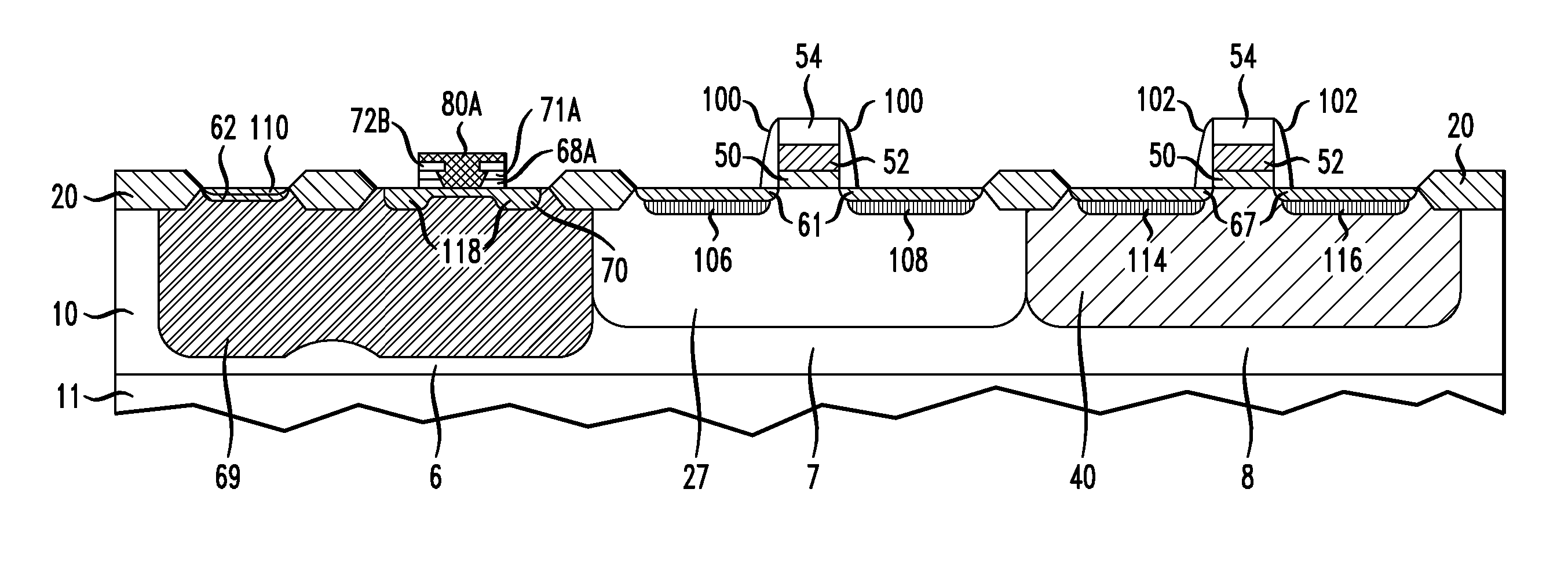
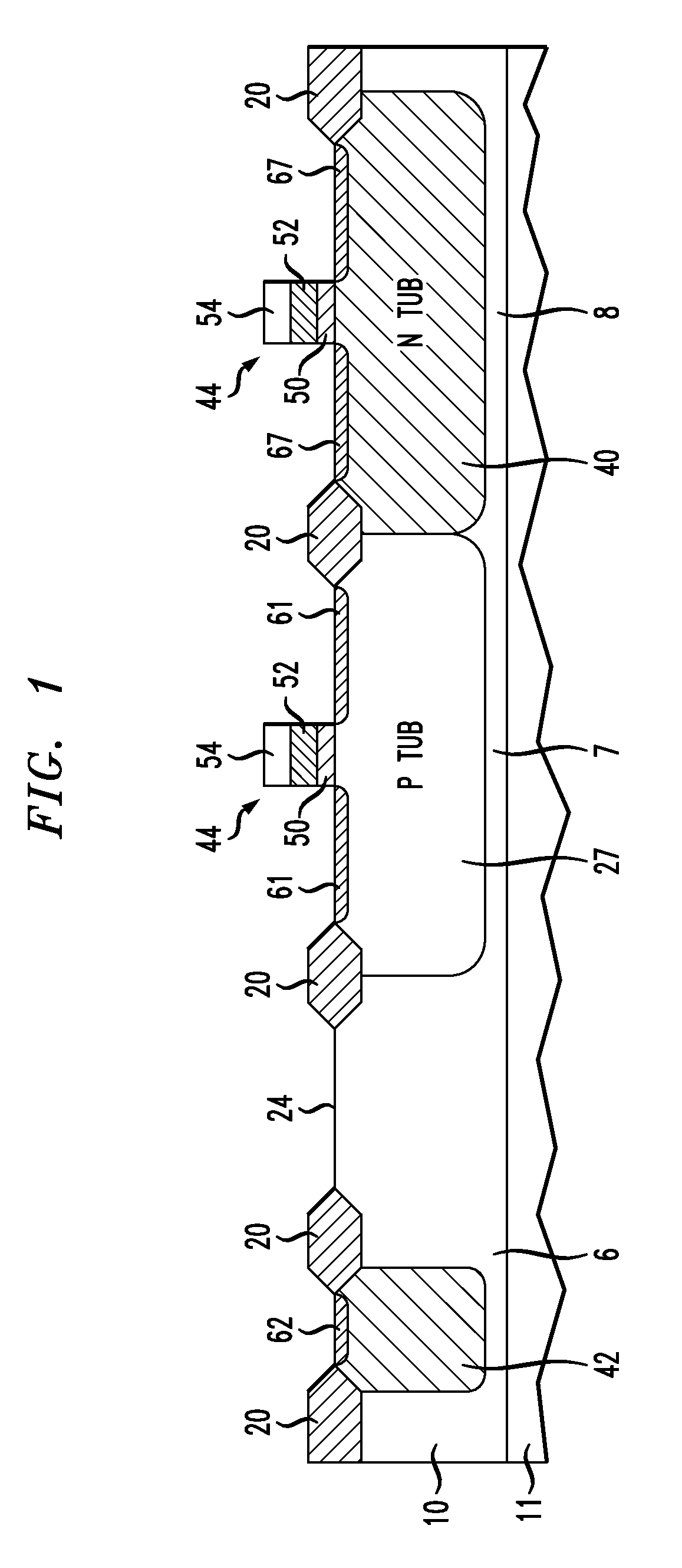
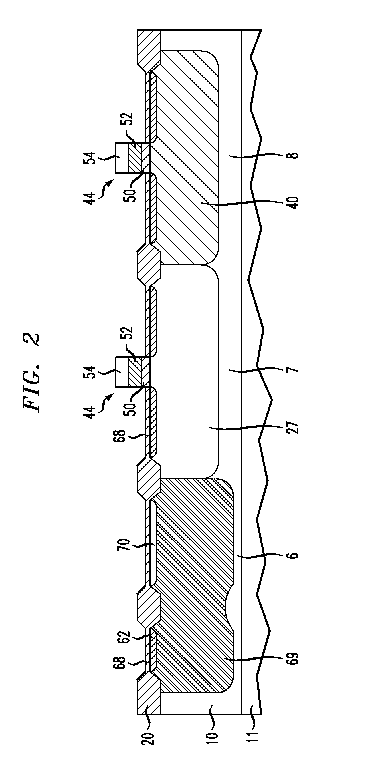
[0015] Before describing in detail an exemplary method for forming bipolar junction transistors and metal-oxide semiconductor field effect transistors according to a thermally stable BiCMOS process of the present invention, it should be observed that the present invention resides primarily in a novel and non-obvious combination of elements and process steps. So as not to obscure the disclosure with details that will be readily apparent to those skilled in the art, certain conventional elements and steps have been presented with lesser detail, while the drawings and the specification describe in greater detail other elements and steps pertinent to understanding the invention.

[0016] The following embodiments are not intended to define limits as to the structure or method of the invention, but only to provide exemplary constructions. The embodiments are permissive rather than mandatory and illustrative rather than exhaustive.

[0017] The teachings of the present invention apply to sili...


PUM


Abstract

A method for forming BiCMOS integrated circuits and structures formed according to the method. After forming doped wells and gate stacks for the CMOS devices and collector and base regions for the bipolar junction transistor, an emitter layer is formed within an emitter window. A dielectric material layer is formed over the emitter layer and remains in place during etching of the emitter layer and removal of the etch mask. The dielectric material layer further remains in place during source / drain implant doping and activation of the implanted source / drain dopants. The dielectric material layer functions as a thermal barrier, to limit out-diffusion of the emitter dopants during the activation step.

Description

FIELD OF THE INVENTION [0001] The present invention relates generally to bipolar junction transistors and more specifically to a thermally stable process for forming bipolar junction transistors and bipolar junction transistors fabricated according to the process. BACKGROUND OF THE INVENTION [0002] Integrated circuits typically comprise semiconductor devices, such as bipolar junction transistors (BJTS) and metal-oxide semiconductor field effect transistors (MOSFETS) formed from doped regions within a semiconductor layer or substrate. Interconnect structures overlying the substrate connect the BJTS and MOSFETS to form circuits. The interconnect structures comprise conductive runners or traces alternating with dielectric layers. Conductive vias disposed in the dielectric layers connect overlying and underlying conductive runners and traces. [0003] BiCMOS integrated circuits comprise both bipolar junction transistors and CMOS (complementary metal oxide semiconductor field effect) trans...

Claims


Application Information

Patent Timeline
Patent Type & Authority Applications(United States)
IPC IPC(8): H01L21/8234
CPCH01L27/0623H01L21/8249
Inventor NANDA, ARUN K.RAGHAVAN, VENKATROSSI, NACE
Owner BELL SEMICON LLC
Why Eureka
Try Eureka