Light emitting element, light emitting device and electronic device

a technology of light emitting devices and light emitting elements, which is applied in the field of light emitting materials, can solve the problems of large power consumption of organic el elements, difficult to use them as medium and small displays, and difficult to manufacture light emitting devices, etc., and achieve the effect of reducing the manufacturing cost of the light emitting device and reducing the power consumption

Inactive Publication Date: 2007-09-06
SEMICON ENERGY LAB CO LTD
View PDF13 Cites 11 Cited by
  • Summary
  • Abstract
  • Description
  • Claims
  • Application Information

AI Technical Summary

Benefits of technology

[0020]Since a light emitting device of the invention includes a light emitting element that can be driven with a low voltage, its power consumption can be

Problems solved by technology

Therefore, inorganic EL elements have large power consumption, so it has been difficult to use

Method used


Image

  • Light emitting element, light emitting device and electronic device
  • Light emitting element, light emitting device and electronic device
  • Light emitting element, light emitting device and electronic device

Examples


embodiment modes

[0036]Hereinafter, embodiment modes of the present invention will be described in detail, with reference to the accompanying drawings. However, the invention is not limited to the description below, and those skilled in the art will appreciate that a variety of modifications can be made to the embodiment modes and their details without departing from the spirit and scope of the invention. Accordingly, the invention should not be construed as being limited to the description of the embodiment modes which follows.

embodiment mode 1

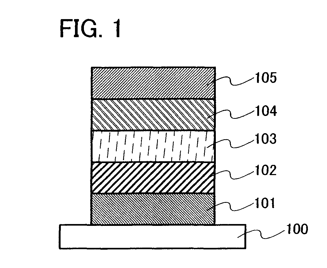
[0037]In this embodiment mode, a thin film light emitting element of the invention will be described with reference to FIG. 1.

[0038]A light emitting element described in this embodiment mode has a structure in which over a substrate 100 are formed a first electrode 101, a second electrode 105, a first insulating layer 102 which is in contact with the first electrode 101, a second insulating layer 104 which is in contact with the second electrode 105, and a light emitting layer 103 which is formed between the first insulating layer 102 and the second insulating layer 104. Light emission is obtained from the light emitting element shown in this embodiment mode when a voltage is applied between the first electrode 101 and the second electrode 105; however, operation is possible with either direct current drive or alternating current drive.

[0039]The substrate 100 is used as a support for the light emitting element. As the substrate 100, glass, plastic, or the like can be used, for examp...

embodiment mode 2

[0052]In this embodiment mode, a thin film light emitting element of the invention will be described with reference to FIG. 2.

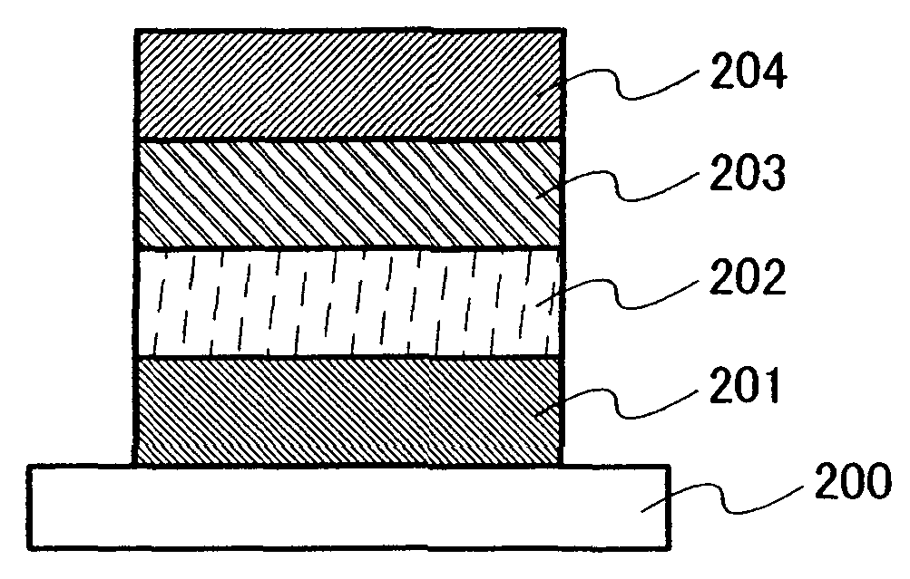
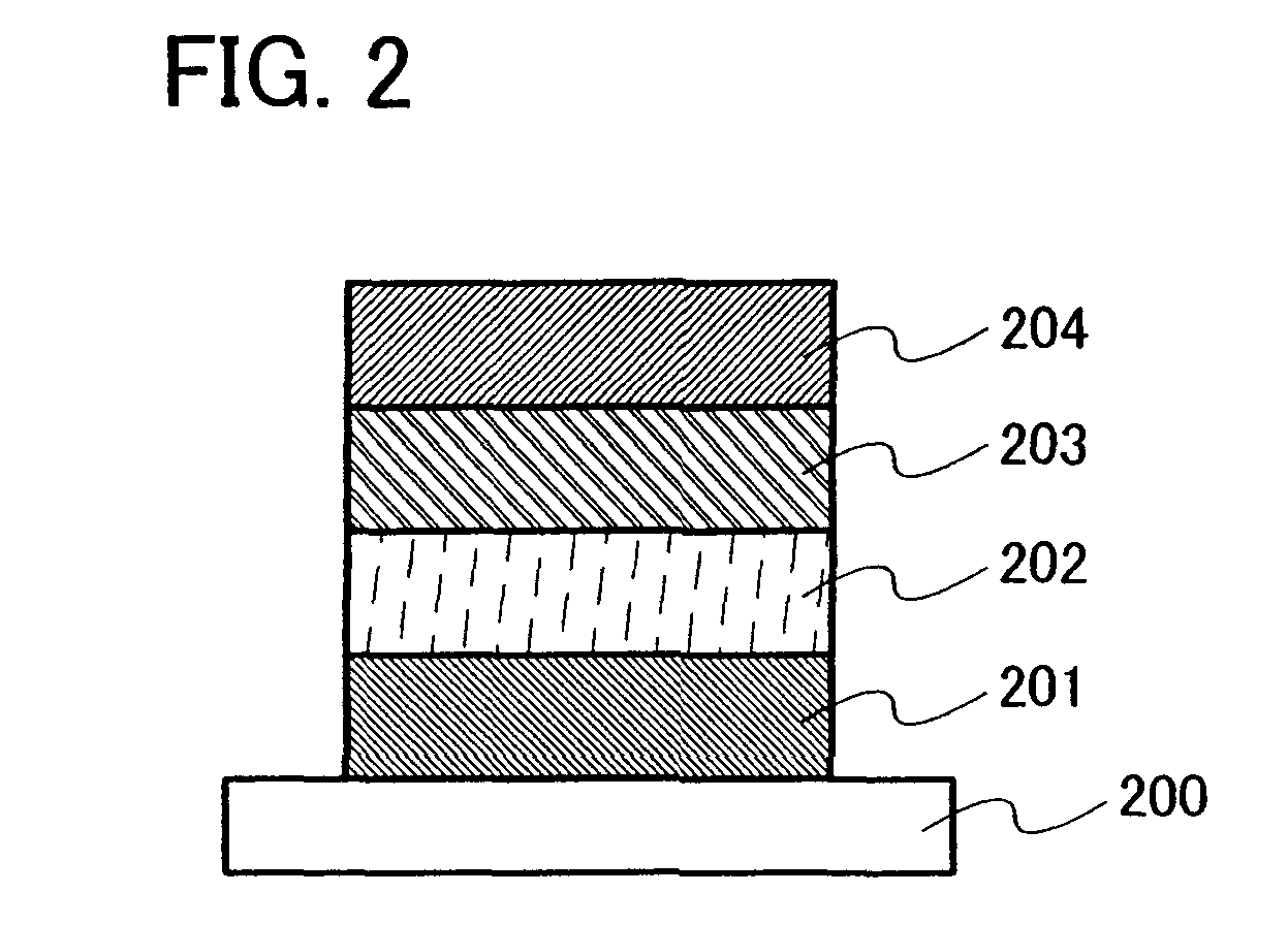
[0053]The light emitting element described in this embodiment mode has a structure which includes a first electrode 201 and a second electrode 204 that are over a substrate 200. Interposed between the first electrode 201 and the second electrode 204 are a semiconductor layer 202 including a chalcopyrite compound, and a light emitting layer 203. In the light emitting element described in this embodiment mode, light emission is obtained by applying a voltage between the first electrode 201 and the second electrode 204; however, the light emitting element can operate using direct current drive or alternating current drive.

[0054]For the substrate 200, the first electrode 201, and the second electrode 204, the same materials as those described in Embodiment Mode 1 can be used. Further, as the semiconductor layer 202 including a chalcopyrite compound, a layer inclu...


PUM


Abstract

A light emitting element that can be driven at a low voltage is provided. Further, a light emitting device and an electronic device with reduced power consumption are provided. A light emitting element is provided that includes a substrate 100, and a first electrode 101, a first insulating layer 102, a light emitting layer 103, a second insulating layer 104, and a second electrode 105, which are over the substrate 100. The light emitting layer 103 includes a compound ABC2, referred to as a ‘chalcopyrite’ (wherein A is Cu or Ag, B is Al, Ga, or In, and C is S, Se, or Te). By employing such a structure, a light emitting element that can be driven at a low voltage can be provided.

Description

TECHNICAL FIELD[0001]The present invention relates to light emitting materials. Further, the present invention relates to light emitting devices that utilize electroluminescence. Moreover, the present invention relates to light emitting devices and electronic devices that have a light emitting element.BACKGROUND ART[0002]In recent years, concerning display devices in televisions, portable telephones, digital cameras and the like, there has been a demand for planar, slim display devices. As display devices which meet this demand, display devices which employ tight emitting elements of a self-luminous type have been a focus of attention. An example of a light emitting element of a self-luminous type is a light emitting element utilizing electroluminescence. Such a light emitting element includes a light emitting material interposed between a pair of electrodes, and light emission can be obtained from the light emitting material by applying a voltage.[0003]Compared to a liquid crystal ...

Claims


Application Information

Patent Timeline
IPC IPC(8): H01L33/00
CPCC09K11/621H05B33/14C09K11/881C09K11/641
Inventor SAKATA, JUNICHIROYOKOYAMA, KOHEIYAMAMOTO, YOSHIAKIKAWAKAMI, TAKAHIRO
Owner SEMICON ENERGY LAB CO LTD
Why Eureka
Try Eureka