Enhancement of remote plasma source clean for dielectric films

a technology of dielectric films and plasma sources, which is applied in the direction of plasma techniques, cleaning of hollow articles, coatings, etc., can solve the problems of recombined oxygen radicals generated by remote plasma sources, damage to chamber components, and undesirable side effects of methods that have been used to remove material originating from other dielectric films, such as non-carbon-containing silicon oxide films

Inactive Publication Date: 2007-09-06
APPLIED MATERIALS INC
View PDF11 Cites 537 Cited by
  • Summary
  • Abstract
  • Description
  • Claims
  • Application Information

AI Technical Summary

Benefits of technology

[0012]The present invention generally relates to methods of cleaning semiconductor processing chambers. Semiconductor processing chambers used to process films comprising carbon and having carbon-containing deposits on their interior surfaces can be cleaned using the methods described herein. For example, semiconductor processing chambers used to process amorphous carbon films, barrier films comprising silicon and carbon, and low dielectric constant films comprising silicon, oxygen, and carbon can be cleaned using the methods described herein.

Problems solved by technology

However, the in situ RF power required to remove the carbon-containing deposits can damage chamber components.
However, many of the oxygen radicals generated by the remote plasma source recombine before sufficient chamber cleaning is achieved.
It has been found that methods that have been used to remove material originating from other dielectric films, such as non-carbon-containing silicon oxide films, may have undesirable side effects and are not always sufficient to remove the carbon from deposits originating from low dielectric constant films having a high carbon content.
For example, it has been observed that cleaning a low dielectric constant organosilicon film deposition chamber by providing in situ radio frequency (RF) power to the chamber to activate sufficient NF3 to clean carbon deposits can result in the formation of contaminating aluminum fluoride particles, since the fluorine ions generated by the RF power can combine with aluminum, which is often used as a lining material in processing chambers.
The removal of contaminating particles from a processing chamber is becoming increasingly important because the device sizes are becoming smaller and aspect ratios are becoming more aggressive.

Method used


Image

  • Enhancement of remote plasma source clean for dielectric films
  • Enhancement of remote plasma source clean for dielectric films
  • Enhancement of remote plasma source clean for dielectric films

Examples


example 1

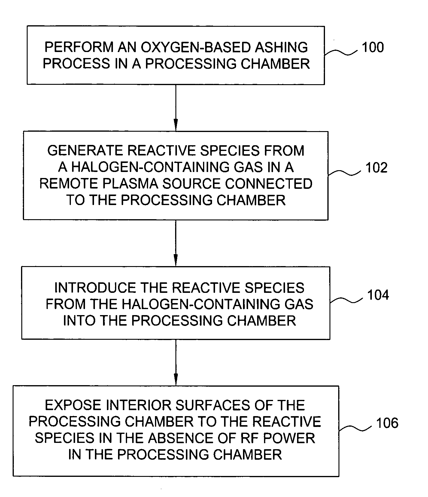
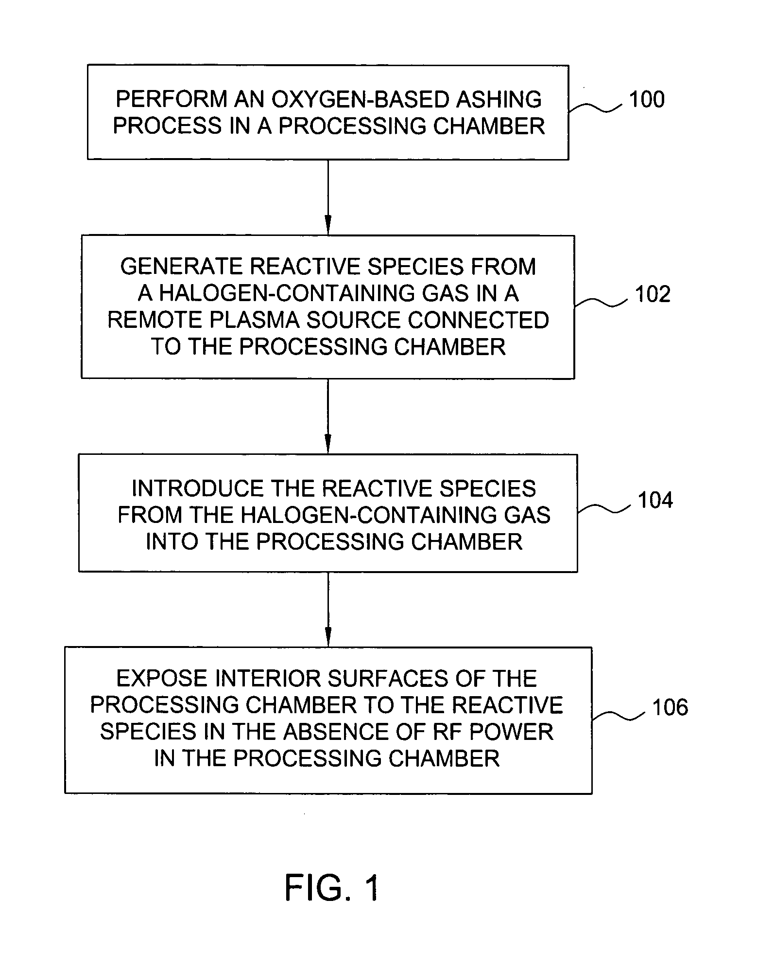
[0067]A PRODUCER® CVD chamber was cleaned by generating reactive oxygen species and reactive fluorine species in an Astron®ex remote plasma source and introducing the reactive oxygen species and reactive fluorine species into the PRODUCER® CVD chamber and exposing the interior surfaces of the chamber to the reactive species for about 150 seconds in the absence of RF power in the chamber to remove about 6000 Å of a low dielectric constant film comprising silicon, oxygen, and carbon. The low dielectric constant film had been previously deposited in the chamber in a PECVD process from a gas mixture comprising methyldiethoxysilane (mDEOS), norbornadiene (BCHD), and oxygen. The reactive oxygen species were introduced into the chamber from the remote plasma source at a flow rate of about 6000 sccm. The reactive fluorine species were introduced into the chamber from the remote plasma source at a flow rate of about 500 sccm. Helium was used as a carrier gas and was flowed into the chamber a...


PUM

PropertyMeasurementUnit
pressureaaaaaaaaaa
pressureaaaaaaaaaa
pressureaaaaaaaaaa

Abstract

Methods for cleaning semiconductor processing chambers used to process carbon-containing films, such as amorphous carbon films, barrier films comprising silicon and carbon, and low dielectric constant films including silicon, oxygen, and carbon are provided. The methods include using a remote plasma source to generate reactive species that clean interior surfaces of a processing chamber in the absence of RF power in the chamber. The reactive species are generated from an oxygen-containing gas, such as O2, and/or a halogen-containing gas, such as NF3. An oxygen-based ashing process may also be used to remove carbon deposits from the interior surfaces of the chamber before the chamber is exposed to the reactive species from the remote plasma source.

Description

CROSS-REFERENCE TO RELATED APPLICATIONS[0001]This application claims the benefit under 35 U.S.C. § 119(e) to provisional application No. 60 / 775,414, filed Feb. 21, 2006, the entire contents of which are incorporated herein by reference.BACKGROUND OF THE INVENTION[0002]1. Field of the Invention[0003]Embodiments of the present invention generally relate to methods of cleaning a processing chamber using a remote plasma source.[0004]2. Description of the Related Art[0005]Integrated circuit geometries have dramatically decreased in size since such devices were first introduced several decades ago. Since then, integrated circuits have generally followed the two year / half-size rule (often called Moore's Law), which means that the number of devices on a chip doubles every two years. Today's fabrication facilities are routinely producing devices having 0.13 μm and even 0.1 μm feature sizes, and tomorrow's facilities soon will be producing devices having even smaller feature sizes.[0006]One o...

Claims


Application Information

Patent Timeline
Patent Type & Authority Applications(United States)
IPC IPC(8): H05H1/24
CPCB08B7/0035H01J37/32862H01J37/32357C23C16/4405B08B9/08
Inventor NOWAK, THOMASYIM, KANG SUBTANG, SUM-YEE BETTYLEE, KWANGDUK DOUGLASNGUYEN, VU NGOC TRANSINGLETON, DENNISSEAMONS, MARTIN JAYJANAKIRAMAN, KARTHIKBALASUBRAMANIAN, GANESHAYOUB, MOHAMEDYEH, WENDY H.DEMOS, ALEXANDROS T.M'SAAD, HICHEM
Owner APPLIED MATERIALS INC
Why Eureka
Try Eureka