Double gate thin-film transistor and method for forming the same

a thin-film transistor and double-gate technology, applied in the field of thin-film transistors, can solve the problems of limiting the suitability of large-area lcd devices, laser annealing, and relatively slow response time of amorphous silicon tft-lcds, and achieve the effect of improving electrical characteristics

Inactive Publication Date: 2007-09-06
IND TECH RES INST
View PDF4 Cites 29 Cited by
  • Summary
  • Abstract
  • Description
  • Claims
  • Application Information

AI Technical Summary

Benefits of technology

[0008]It is a primary object of the present invention to provide a double gate thin-film transistor using

Problems solved by technology

However, the carrier mobility in an amorphous silicon film is much lower than that in a poly-silicon film, so that conventional amorphous silicon TFT-LCDs exhibit a relatively slow response time that limits their suitability for large-area LCD devices.
Though there have been lots of reports on converting low-temperature grown amorphous sili

Method used


Image

  • Double gate thin-film transistor and method for forming the same
  • Double gate thin-film transistor and method for forming the same
  • Double gate thin-film transistor and method for forming the same

Examples


Embodiment Construction

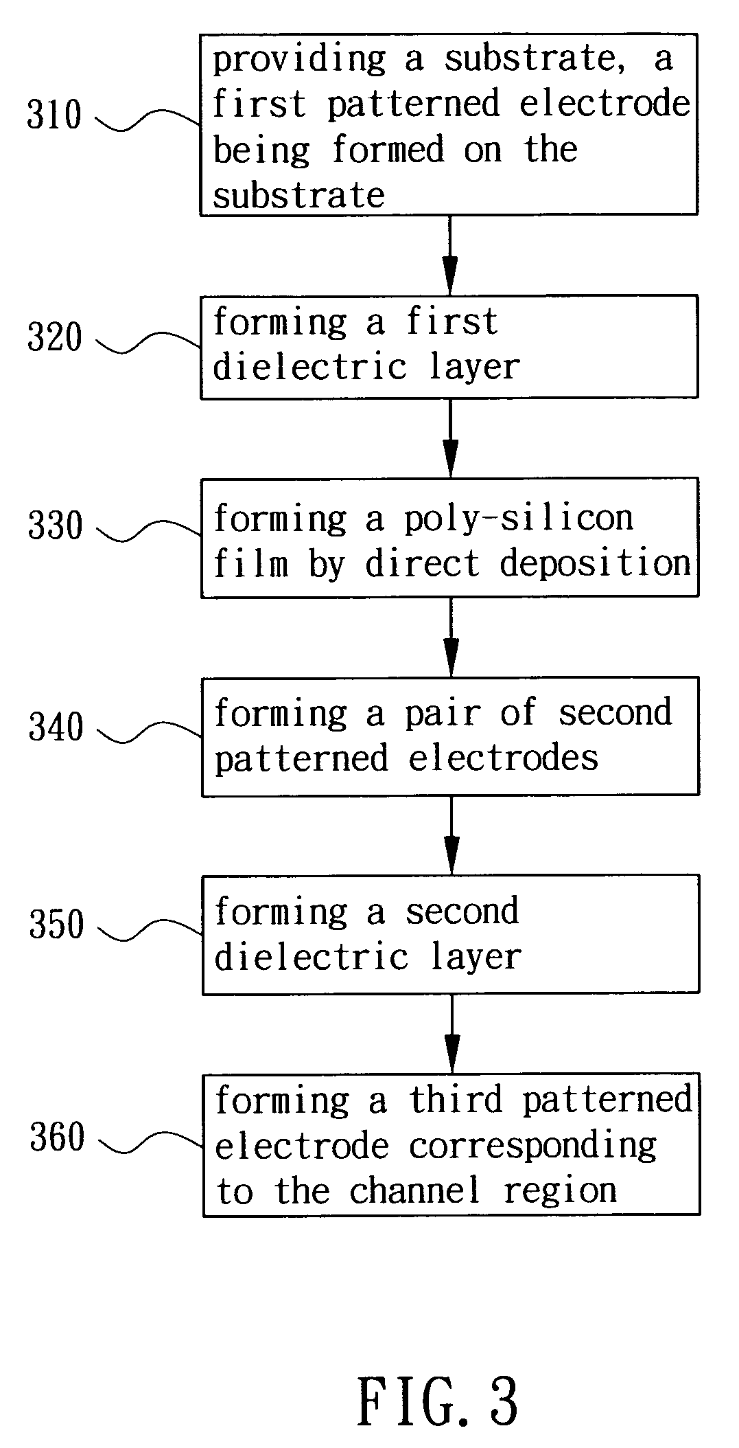
[0027]The present invention providing a double gate thin-film transistor and a method for forming the same can be exemplified by the preferred embodiment as described hereinafter.

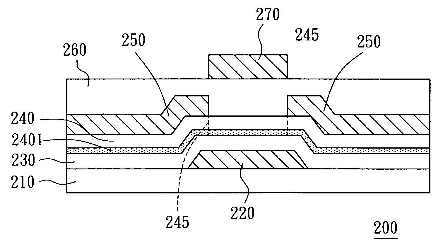
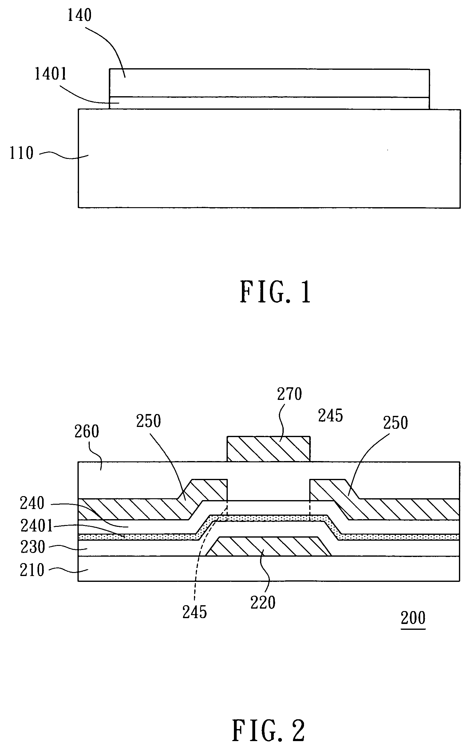
[0028]Please refer to FIG. 2, which is a cross-sectional view of a double-gate thin-film transistor according to the present invention. In the present invention, the double-gate thin-film transistor 200 comprises: a first patterned electrode 220 formed on a substrate 210; a first dielectric layer 230, covering the first patterned electrode 220 and the substrate 210; a poly-silicon film 240, formed by direct deposition on the first dielectric layer 230 so as to form between the poly-silicon film 240 and the first dielectric layer 230 an incubation layer 2401 comprising amorphous silicon; a pair of second patterned electrodes 250, formed on the poly-silicon film 240 so as to define in the poly-silicon film 240 and the incubation layer 2401 between the second patterned electrodes 250 a channel region 245 corre...


PUM


Abstract

A double-gate thin-film transistor and a method for forming the same, using low-temperature poly-silicon formed by direct deposition on a substrate so as to simplify the manufacturing process and improve the electrical characteristics. The double-gate thin-film transistor comprises: a first patterned electrode formed on a substrate; a first dielectric layer; a poly-silicon film, formed by direct deposition on the first dielectric layer so as to form between the poly-silicon film and the first dielectric layer an incubation layer comprising amorphous silicon; a pair of second patterned electrodes, formed on the poly-silicon film so as to define in the poly-silicon film and the incubation layer between the second patterned electrodes a channel region corresponding to the first patterned electrode; a second dielectric layer; and a third patterned electrode corresponding to the channel region. The method comprises steps of: providing a substrate, a first patterned electrode being formed on the substrate; forming a first dielectric layer; forming a poly-silicon film by direct deposition on the first dielectric layer so as to form between the poly-silicon film and the first dielectric layer an incubation layer comprising amorphous silicon; forming a pair of second patterned electrodes on the poly-silicon film so as to define in the poly-silicon film and the incubation layer between the second patterned electrodes a channel region corresponding to the first patterned electrode; forming a second dielectric layer; and forming a third patterned electrode corresponding to the channel region.

Description

BACKGROUND OF THE INVENTION[0001]1. Field of the Invention[0002]The present invention generally relates to a thin-film transistor and a method for forming the same and, more particularly, to a double gate thin-film transistor and a method for forming the thin-film transistor, using a poly-silicon film by direct deposition at low temperatures so as to simply the processing and improve electrical characteristics.[0003]2. Description of the Prior Art[0004]In semiconductor manufacturing, since the amorphous silicon film can be deposited on a glass substrate at low temperatures, thin-film transistors (TFTs) comprising amorphous silicon are widely used in the field of liquid crystal displays (LCDs).[0005]However, the carrier mobility in an amorphous silicon film is much lower than that in a poly-silicon film, so that conventional amorphous silicon TFT-LCDs exhibit a relatively slow response time that limits their suitability for large-area LCD devices. Though there have been lots of repor...

Claims


Application Information

Patent Timeline
IPC IPC(8): H01L21/84H01L21/00
CPCH01L29/78648H01L29/6675
Inventor WANG, LIANG-TANGWANG, MIN-CHUANGPENG, I-HSUAN
Owner IND TECH RES INST
Why Eureka
Try Eureka