Charge storage structure formation in transistor with vertical channel region

a transistor and vertical channel technology, applied in the field of semiconductor devices, can solve problems such as the possibility of charge moving between charge storage locations

Inactive Publication Date: 2007-09-13
NXP USA INC
View PDF15 Cites 447 Cited by
  • Summary
  • Abstract
  • Description
  • Claims
  • Application Information

AI Technical Summary

Problems solved by technology

One problem with some multi-bit cells with a charge storage structure having multiple charge storage locations is that the charge may migrate between the charge storage locations, especially with a higher conductivity of some charge storage structure material.

Method used


Image

  • Charge storage structure formation in transistor with vertical channel region
  • Charge storage structure formation in transistor with vertical channel region
  • Charge storage structure formation in transistor with vertical channel region

Examples


Embodiment Construction

[0015] The following sets forth a detailed description of a mode for carrying out the invention. The description is intended to be illustrative of the invention and should not be taken to be limiting.

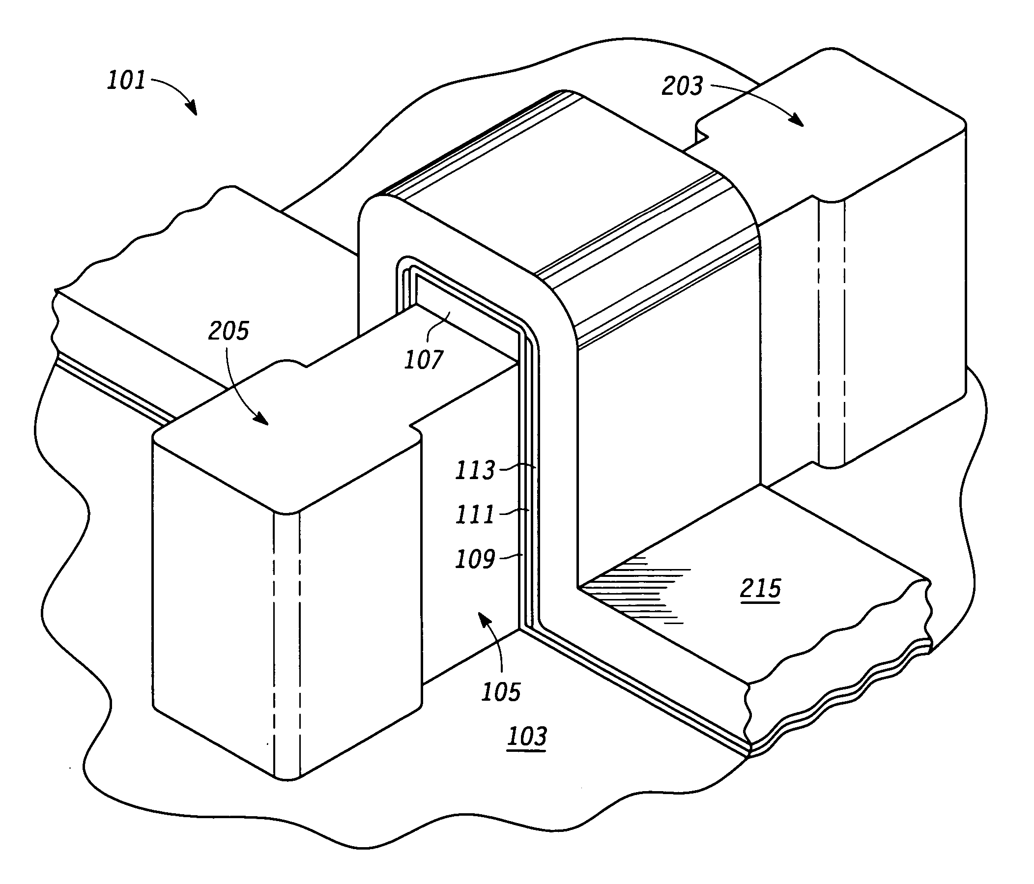
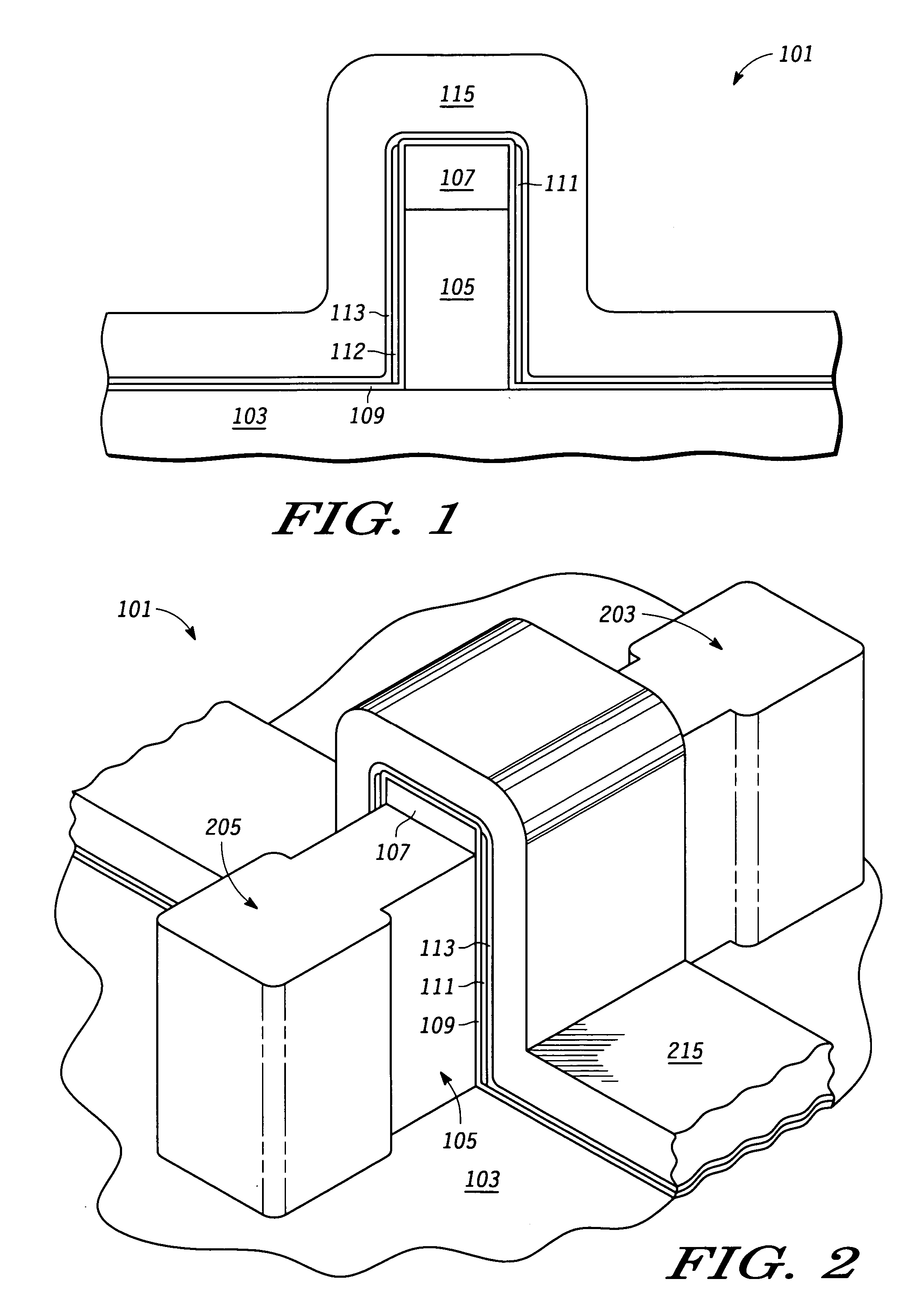
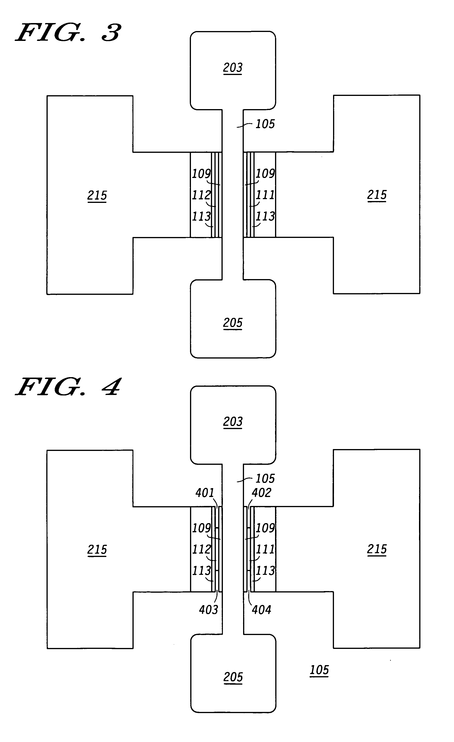
[0016]FIG. 1 is a partial side cross sectional side view of a wafer utilized to form a multi-bit memory cell according to one embodiment of the present invention. Wafer 101 includes an insulating layer 103. In one embodiment, layer 103 is located over a semiconductor substrate (not shown). A semiconductor fin structure 105 and cap 107 are formed by pattering a semiconductor layer (not shown) and dielectric layer (e.g. oxide, silicon nitride) (not shown) over the semiconductor layer. In one embodiment, fin structure 105 is monocrystalline silicon but may be of other semiconductor materials (e.g. silicon germanium) in other embodiments. Also, cap 107 may be of other materials in other embodiments.

[0017] After the patterning to form fin structure 105 and cap 107, a dielectric layer 109 i...


PUM


Abstract

A semiconductor device includes a semiconductor structure having a first sidewall. A vertical channel region is formed in the semiconductor structure along the first sidewall between a first current electrode region and a second current electrode region. First and second charge storage structures are formed adjacent to the first sidewall in openings of a dielectric layer. The first and second charge storage structures are electrically isolated from each other and from the semiconductor structure. A control electrode is formed adjacent to the first sidewall. In another embodiment, third and fourth charge storage structures may be formed adjacent to a second sidewall of the semiconductor structure in openings of a dielectric layer.

Description

BACKGROUND OF THE INVENTION [0001] 1. Field of the Invention [0002] This invention relates in general to semiconductor devices and specifically to non volatile memory devices. [0003] 2. Description of the Related Art [0004] Non volatile memory devices utilize charge storage structures for selectively storing charge indicative of a bit of information to be stored. Such charge storage structures may include nitride, silicon nanocrystals, semiconductor material, or conductive material e.g. metals. [0005] Some memories utilize multi-bit (multiple bit) memory cells. A multi-bit memory cell is a cell that can store more than one bit of information. Some multi-bit cells include a charge storage structure that has multiple charge storage locations or regions in the charge storage structure. Charge is selectively added to each region to selectively store a bit in the cell. [0006] One problem with some multi-bit cells with a charge storage structure having multiple charge storage locations is...

Claims


Application Information

Patent Timeline
Patent Type & Authority Applications(United States)
IPC IPC(8): H01L29/76
CPCH01L29/66825H01L29/66833H01L29/7926H01L29/7887H01L29/7923H01L29/785
Inventor ORLOWSKI, MARIUS
Owner NXP USA INC
Why Eureka
Try Eureka