Semiconductor device having silicon-diffused metal wiring layer and its manufacturing method
a semiconductor and metal wiring technology, applied in the direction of semiconductor devices, semiconductor/solid-state device details, electrical apparatus, etc., can solve the problems of reducing the manufacturing yield, enhancing the electromigration, and delay the propagation of signals on the wiring layer, so as to achieve the effect of decreasing the resistan
- Summary
- Abstract
- Description
- Claims
- Application Information
AI Technical Summary
Benefits of technology
Problems solved by technology
Method used
Image


Examples
first embodiment
[0081]FIGS. 5A through 5J are cross-sectional views for explaining the method for manufacturing a semiconductor device according to the present invention. In this case, a one-layer single-damascene structure is formed.
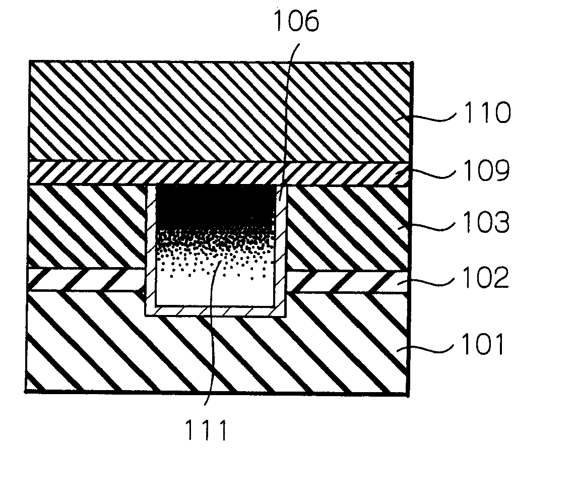
[0082] First, referring to FIG. 5A, in the same way as in FIG. 1A, an insulating underlayer 101 made of silicon dioxide or the like is formed on a silicon substrate (not shown) where various semiconductor elements are formed. Then, an about 50 nm thick etching stopper 102 made of SiCN is formed by a plasma process on the insulating underlayer 101. Then, an about 400 nm thick insulating interlayer 103 made of silicon dioxide is deposited by a plasma CVD process on the etching stopper 102. Then, an anti-reflective coating layer 104 and a photoresist layer 105 are sequentially coated on the insulating interlayer 103. Then, the photoresist layer 105 is patterned by a photolithography process, so that a groove 105a is formed in the photoresist layer 105. Note that the insul...
second embodiment
[0125]FIGS. 9A through 9S are cross-sectional views for explaining the method for manufacturing a semiconductor device according to the present invention. In this case, a two-layer single-damascene structure is formed.
[0126] Assume that the semiconductor device as illustrated in FIG. 5J is completed. In this case, the silicon-diffused copper layer 111 serves as a lower wiring layer.
[0127] Next, referring to FIG. 9A, an anti-reflective coating layer 131 and a photoresist layer 132 are sequentially coated on the insulating interlayer 110. Then, the photoresist layer 132 is patterned by a photolithography process, so that a via hole 132a is formed in the photoresist layer 132.
[0128] Next, referring to FIG. 9B, the insulating interlayer 110 and the anti-reflective coating layer 131 is etched by a dry etching process using the photoresist layer 132 as a mask. In this case, since the copper diffusion barrier layer 109 is an incomplete etching stopper, the copper diffusion barrier layer ...
third embodiment
[0197]FIGS. 10A through 10V are cross-sectional views for explaining the method for manufacturing a semiconductor device according to the present invention. In this case, a two-layer via first type dual-damascene structure is formed.
[0198] First, referring to FIG. 10A, an insulating underlayer 201 made of silicon dioxide or the like is formed on a silicon substrate (not shown) where various semiconductor elements are formed. Then, an about 50 nm thick etching stopper 202 made of SiCN is formed by a plasma process on the insulating layer 201. Then, an about 300 nm thick insulating interlayer 203a made of a low-k material such as SiOF, SiOC, organic material or inorganic material such as ladder-type hydrogen siloxane having a lower dielectric constant than that of silicon dioxide is coated on the etching stopper 202. Then, an about 100 nm thick mask insulating layer 203b made of silicon dioxide is deposited by a plasma CVD process on the insulating interlayer 203a. Then, an anti-refle...
PUM
| Property | Measurement | Unit |
|---|---|---|
| density | aaaaa | aaaaa |
| refractive index | aaaaa | aaaaa |
| temperature | aaaaa | aaaaa |
Abstract
Description
Claims
Application Information
 - R&D
- Intellectual Property
- Life Sciences
- Materials
- Tech Scout
- Unparalleled Data Quality
- Higher Quality Content
- 60% Fewer Hallucinations
Browse by: Latest US Patents, China's latest patents, Technical Efficacy Thesaurus, Application Domain, Technology Topic, Popular Technical Reports.
© 2025 PatSnap. All rights reserved.Legal|Privacy policy|Modern Slavery Act Transparency Statement|Sitemap|About US| Contact US: help@patsnap.com