

Method of manufacturing semiconductor device
a manufacturing method and semiconductor technology, applied in the direction of liquid/solution decomposition chemical coating, coating, metallic material coating process, etc., can solve the problem of carbon dioxide being inevitably generated on scrapping
- Summary
- Abstract
- Description
- Claims
- Application Information
AI Technical Summary
Problems solved by technology
Method used
Image

Examples
embodiment 1
[0078]A combination of two kinds of rinsing liquids (naphthalene-based solvent and α-pinene) was employed for the EBR and the back-rinsing to investigate throughput and profitability. The throughput can be assessed by estimating the time required for performing the EBR and for the drying after the back-rinsing.
[0079]The throughput can be determined from the drying characteristics of the rinsing liquid. The higher the vapor pressure of the rinsing liquid is, the faster the drying speed of the rinsing liquid would become. Therefore, the vapor pressure of the rinsing liquid should preferably be 1 hPa or more. As long as the rinsing liquid has a vapor pressure of 1 hPa or more, the time required for drying the rinsing liquid after the step of back-rinsing can be shortened to 10 seconds or less. Whereas, when a naphthalene-based solvent which is inferior in drying characteristics is employed in the back-rinsing, the throughput would deteriorate.
[0080]However, since the width of edge-cutt...
embodiment 2
[0084]In this embodiment, α-d-pinene having a purity of 97% or more was employed as a rinsing liquid to form a coated insulating film comprising PHPS. As a coating liquid to be used in this case, a solution was prepared by dissolving the same kind of PHPS as employed in the aforementioned preliminary experiment 1 in di-n-butyl ether.
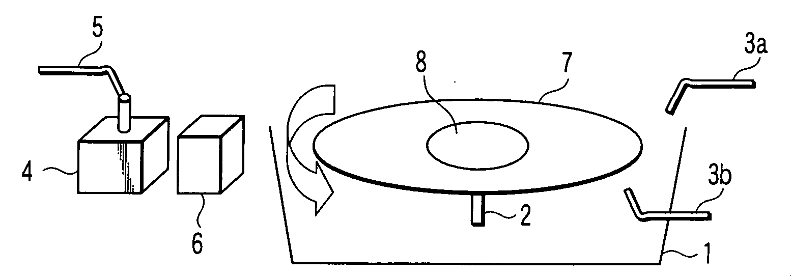
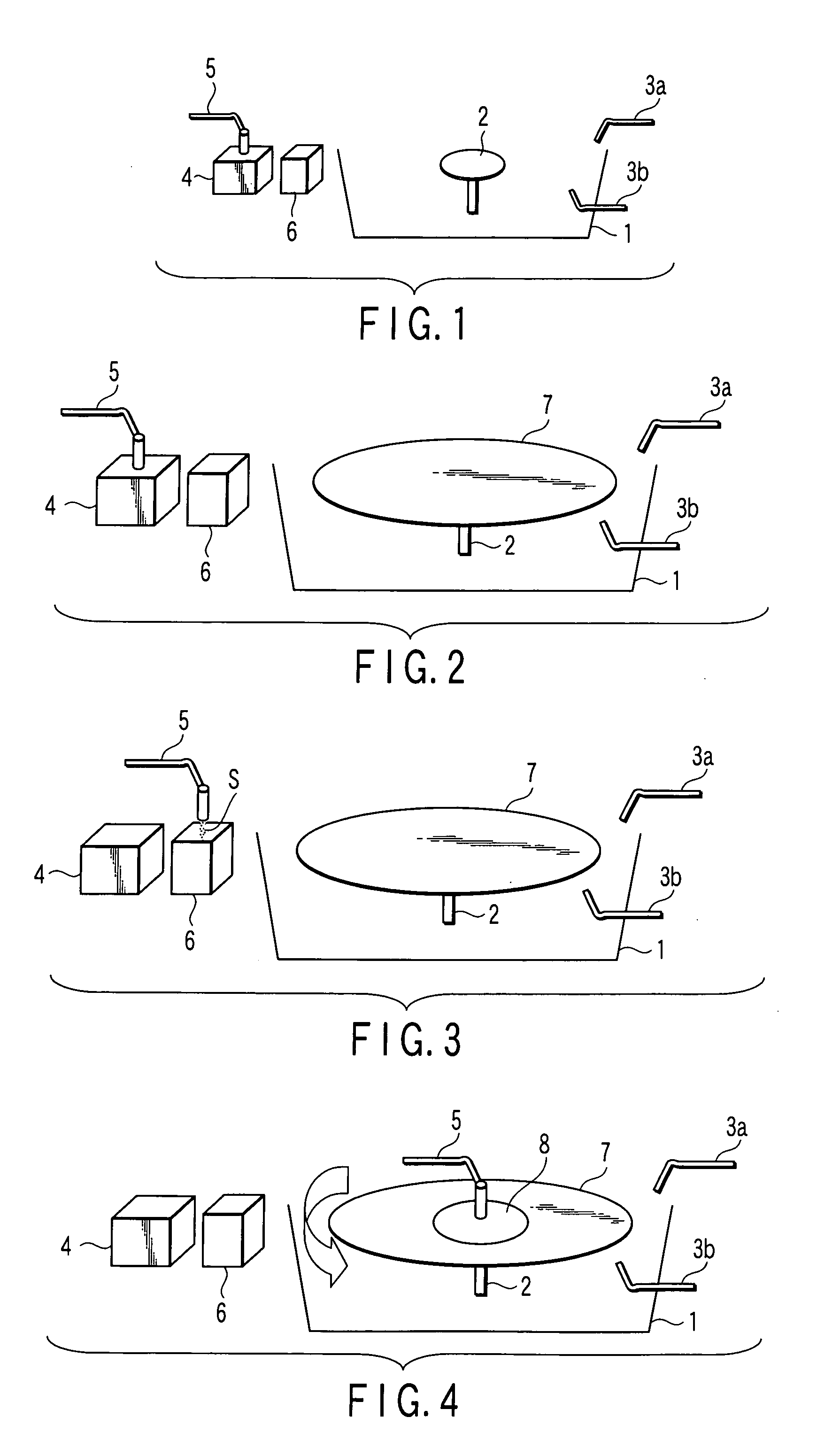
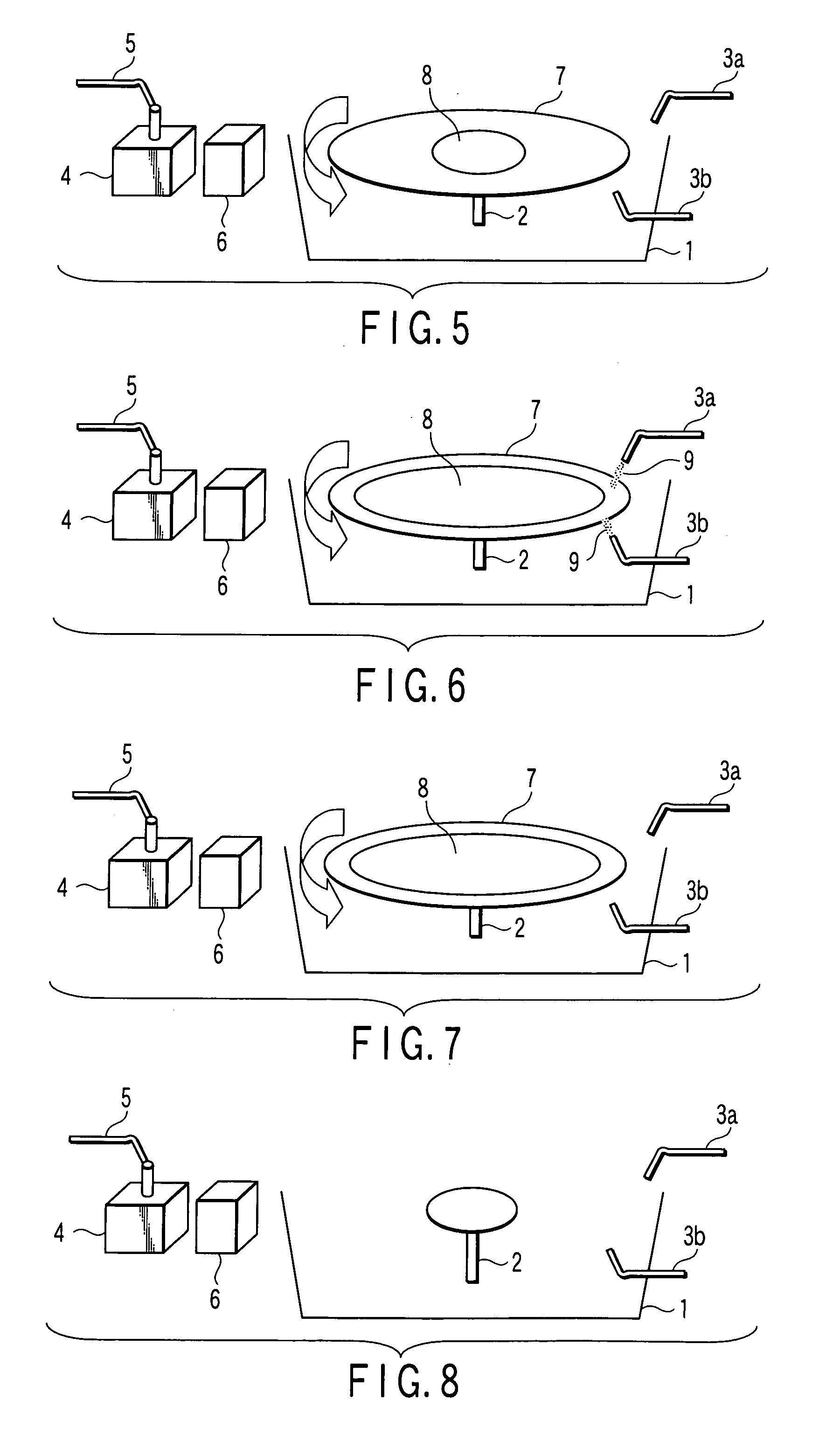
[0085]The process recipe for coating and the time required for each of the steps are shown in the following Table 4. First of all, as shown in FIG. 2, a wafer 7 is mounted on a spin chuck 2 provided inside a coater cup 1. Then, as shown in FIG. 3, a chemicals nozzle 5 is taken out of a solvent bath 4 and a dummy dispense (delivery) is performed for a short time, thus replacing the coating liquid existing in a distal end of nozzle by a flesh coating liquid. This flesh coating liquid is then delivered by applying a pressure to the interior of chemicals tube using a high-pressure gas or forcedly delivered using a liquid transfer pump. (In Table 4, details a...
embodiment 3
[0090]Next, one embodiment of a shallow trench isolation (STI) embedding method will be explained. A process of manufacturing a memory cell of CMOS structure will be explained with reference to FIGS. 9 to 12.
[0091]First of all, a silicon dioxide film (about 10 nm in thickness) 11 is formed on the surface of a silicon substrate 10 by thermal oxidation method. Then, as a CMP stopper film, a silicon nitride film (about 200 nm in thickness) 12 is formed on the silicon dioxide film 11 by the vacuum CVD method. The film thickness to be formed on the substrate can be optionally altered. For example, the film thickness of the silicon nitride film 12 may be selected from the range of 100-300 nm.
[0092]By photolithography and the dry etching method, an element-isolating trench (STI trench) 13 having a depth penetrating through the CMP stopper film 12 and the silicon dioxide film 11 and reaching to the silicon substrate 10 is formed as shown in FIG. 9. The width and depth of the STI trench 13 m...
PUM
| Property | Measurement | Unit |
|---|---|---|
| temperature | aaaaa | aaaaa |
| temperature | aaaaa | aaaaa |
| time | aaaaa | aaaaa |
Abstract
Description
Claims
Application Information