

Plasma processing apparatus
a technology of processing apparatus and plasma, which is applied in the direction of electrical apparatus, electric discharge tubes, basic electric elements, etc., can solve the problem of continuously produced defective devices
- Summary
- Abstract
- Description
- Claims
- Application Information
AI Technical Summary
Benefits of technology
Problems solved by technology
Method used
Image

Examples
first embodiment
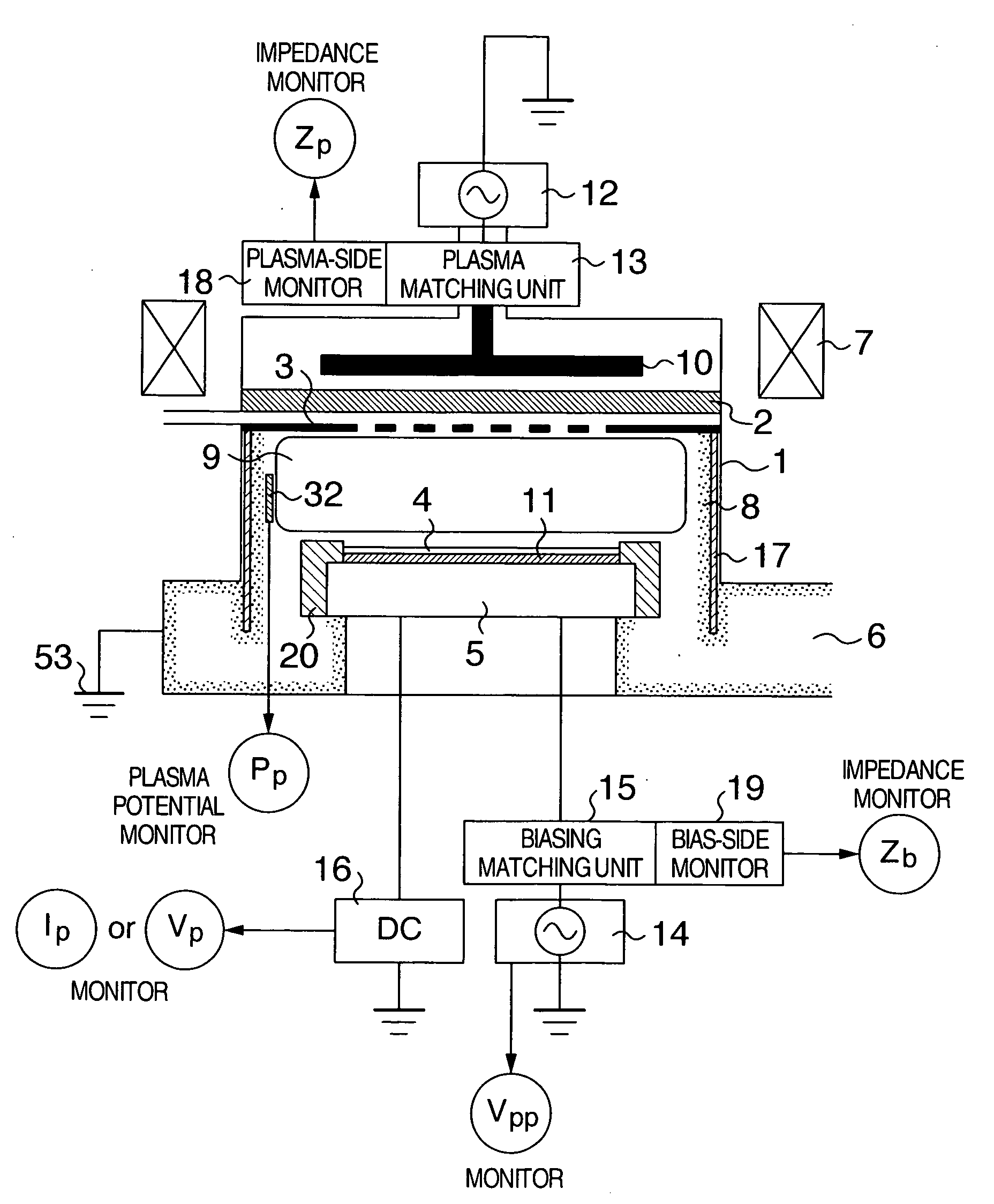
[0034]FIG. 1 is a diagram to explain a first embodiment of a plasma processing apparatus. In the example of FIG. 1, a plasma etching apparatus using electromagnetic waves in an Ultra-High Frequency (UHF) band is employed as the plasma processing apparatus.
[0035]In the upper section of a vacuum chamber 1 for plasma processing, a dielectric vacuum window 2 to introduce an electromagnetic wave in the UHF band to generate plasma and a dielectric gas injection plate 3 to introduce reactive processing gas are disposed. Reaction products resultant from the etching process are discharged from an outlet 6 in the lower section of the chamber 1. On a side-wall section inside the chamber 1, there are arranged cylindrical inner parts 17 including a base metal of aluminum and an inner wall protective coating 8 applied on a surface of the base metal using a dielectric material. A wafer (sample) 4 to be etched is placed on an electrostatic chuck constructed by disposing a wafer attracting coating f...
second embodiment
[0056]In conjunction with the second embodiment, description will be given of an example in which a abnormality occurs in the vicinity of the sample stage 5 disposed in the lower section of the chamber 1 or the susceptor 20 covering the periphery of the sample stage in the plasma processing apparatus shown in FIG. 1.
[0057]The mass-production is carried out while monitoring four values of Zp, Zb, Vpp, and Ip in the plasma processing apparatus of FIG. 1. The condition for the mass-production includes “cleaning condition” and “etching condition” as in the first embodiment. During the operation to monitor the four monitor values, each time about ten thousand wafers are processed, the pulsating variation appears in Ip and the insulation breakdown takes place in the inner wall protective coating 8 on the surface of the cylindrical inner parts 17 as described in conjunction with the first embodiment. To cope with the difficulty, the mass-production is continuously carried out by periodical...
third embodiment
[0064]In conjunction with the third embodiment, description will be given of an example in which an abnormality occurs in the plasma processing apparatus of FIG. 1 in the vicinity of the vacuum window 2 disposed in the upper section of the chamber 1 to introduce the plasma generating power and the gas injection plate 3 disposed in the upper section of the chamber 1 to introduce the reactive processing gas.
[0065]The mass-production is carried out in the plasma processing apparatus of FIG. 1 while monitoring four values of Zp, Zb, Vpp, and Ip. The condition for the mass-production includes “cleaning condition” and “etching condition” as in the first embodiment. In the state shown in the second embodiment, the mass-production is continuously conducted. The four monitor values are monitored as above also after 200000 wafers are processed. The pulsating variation appears in Ip each time about ten thousand wafers are processed as described in conjunction with the first and second embodime...
PUM
| Property | Measurement | Unit |
|---|---|---|
| pressure | aaaaa | aaaaa |
| time | aaaaa | aaaaa |
| dc current | aaaaa | aaaaa |
Abstract
Description
Claims
Application Information