Multi-layered thermal sensor for integrated circuits and other layered structures

a technology of integrated circuits and layers, applied in the direction of heat measurement, instruments, semiconductor/solid-state device details, etc., can solve the problems of sensor not being able to be integral parts of the circuit being measured, sensor being more susceptible to variations in the wire fabrication process, sensor not being able to be placed at the particular location, etc., to achieve the effect of increasing the utility of the space in the i

Inactive Publication Date: 2007-09-20
IBM CORP
View PDF30 Cites 8 Cited by
  • Summary
  • Abstract
  • Description
  • Claims
  • Application Information

AI Technical Summary

Benefits of technology

[0009] The invention is directed to a compact thermal sensor for an integrated circuit or other multi-layered structure, as described hereinafter, wherein prior art problems of the above type are overcome by placing different components of the sensor on two or more different metal layers of the IC or other structure. This allows the lateral area needed for the sensor resistance wire on any particular layer to be selectively reduced. Moreover, other wires not related to the sensor are allowed to pass through the sensor component on a given IC layer, and such wires can be shielded laterally. Thus, the above configuration provides a thermal sensor for an IC that significantly increases utility of space in the IC.

Problems solved by technology

However, this arrangement has a number of drawbacks.
Thus, the sensor configuration can significantly reduce the wiring channels on that layer and hence, the sensor cannot be an integral part of a circuit being measured.
For example, there could be concern of a hot spot developing at a particular IC location, due to substantial power dissipation.
However, because of the limitations of currently available sensors, it could be difficult to place one of such sensors at the particular location, in order to monitor location temperature.
In a prior art thermal sensor of the above type, there are conflicting requirements in that the sensor wire needs to be narrow enough to provide enough resistance over-all, but must still be wide enough that the sensor itself does not generate heat.
Also, the use of narrow width lines or wires makes the sensor more susceptible to variations in the wire fabrication process, since process variations tend to vary by some percentage around a mean value.
If the value is too high, the value cannot be measured by available measurement tools.
If the resistance is too low, it becomes too insensitive.
Process variations limit how close the design can be made to the high side of the optimum resistance range.

Method used


Image

  • Multi-layered thermal sensor for integrated circuits and other layered structures
  • Multi-layered thermal sensor for integrated circuits and other layered structures
  • Multi-layered thermal sensor for integrated circuits and other layered structures

Examples


Embodiment Construction

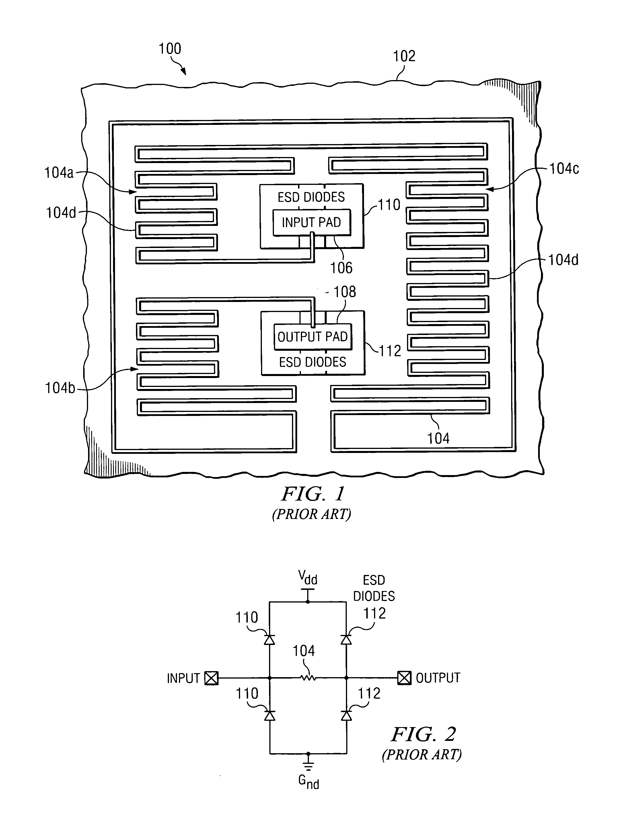
[0021] Referring to FIG. 1, there is shown a prior art resistive thermal sensor of the type described above, formed on a metal layer 102 of an IC semiconductor that is not otherwise shown. Sensor 100 comprises a continuous wire or line 104 formed of conductive metal. Herein, the terms “wire”, “line” and “trace” are used interchangeably, to refer to a narrow conductive path formed on one of the metal layers of an IC.

[0022] As discussed above, wire 104 must be of substantial length in order to have a resistance that is high enough to be useful in determining temperature adjacent to sensor 100. Thus, in order to provide sufficient wire length, wire 104 is placed on layer 102 in a serpentine pattern, as shown by FIG. 1 and discussed above. The pattern comprises several larger loops 104a, 104b and 104c, wherein each of the larger wire loops comprises a number of smaller or tighter wire loops 104d. As stated above, sensor wire 104 must be narrow enough to have sufficient resistance over ...


PUM


Abstract

A compact resistive thermal sensor is provided for an integrated circuit (IC), wherein different sensor components are placed on different layers of the IC. This allows the lateral area needed for the sensor resistance wire on any particular IC layer to be selectively reduced. In a useful embodiment, a plurality of first linear conductive members are positioned in a first IC layer, in spaced-apart parallel relationship with one another. A plurality of second linear conductive members are similarly positioned in a second IC layer in spaced-apart parallel relationship with one another, and in orthogonal relationship with the first linear members or in parallel with existing wiring channels of the second IC layer. Conductive elements respectively connect the first linear members into a first conductive path, and the second linear members into a second conductive path. A third conductive element extending between the first and second layers connects the first and second conductive paths into a single continuous conductive path, wherein the path has a resistance that varies with temperature. A device responsive to an electric current sent through the continuous path determines temperature of the path from the path resistance. Two or more of the thermal sensors could be connected in series, for use in measuring critical IC circuits.

Description

BACKGROUND OF THE INVENTION [0001] 1. Field of the Invention [0002] The invention disclosed and claimed herein generally pertains to a compact thermal sensor apparatus for monitoring temperature in an integrated circuit (IC) or other semiconductor package. More particularly, the invention pertains to sensor apparatus of the above type that comprises two or more components, wherein each component is located on a different layer of the IC. Even more particularly, the invention pertains to a sensor apparatus of the above type wherein wiring channels for IC functions unrelated to the thermal sensor can readily be routed through any of the sensor components. [0003] 2. Description of the Related Art [0004] It is generally important to monitor the internal temperature of an integrated circuit such as a microprocessor or the like. Typically, an analog thermal sensor for integrated circuits comprises a metal line or wire of substantial length and a fixed width. From the designed length of th...

Claims


Application Information

Patent Timeline
Patent Type & Authority Applications(United States)
IPC IPC(8): H01L31/058
CPCG01K7/16G01K1/14
Inventor RAHMAN, AQUILURWALLS, LLOYD ANDRE
Owner IBM CORP
Why Eureka
Try Eureka