Novel chip packaging structure for improving reliability

a packaging structure and chip technology, applied in the field of flip chip packaging, can solve the problems of affecting the chip, requiring a large number of solder bumps, crowding of solder bumps along the perimeter of the flip chip, etc., to reduce thermally induced delamination stresses, reduce stress, and dissipate heat from the flip chip

Active Publication Date: 2007-09-20
TAIWAN SEMICON MFG CO LTD
View PDF7 Cites 30 Cited by
  • Summary
  • Abstract
  • Description
  • Claims
  • Application Information

AI Technical Summary

Benefits of technology

[0015] In accordance with these and other objects and advantages, the present invention is generally directed to a novel IC chip package structure having an IC flip chip or die bonded to a carrier substrate. An adhesive material such as epoxy is sandwiched between the flip chip and the carrier substrate. Multiple concave stress-relieving structures, such as a set of stress relief openings or slots or a channel matrix, for example, are provided in the backside of the IC flip chip. During thermal testing and/or functioning of the flip chip, the concave structures reduce stresses between the flip chip and the ca...

Problems solved by technology

Consequently, ambient air is able to penetrate the package and adversely affect the chip over time.
Because of the numerous functions typically performed by the microcircuitry of a flip chip, a relatively large number of solder bumps a...

Method used


Image

  • Novel chip packaging structure for improving reliability
  • Novel chip packaging structure for improving reliability
  • Novel chip packaging structure for improving reliability

Examples


Embodiment Construction

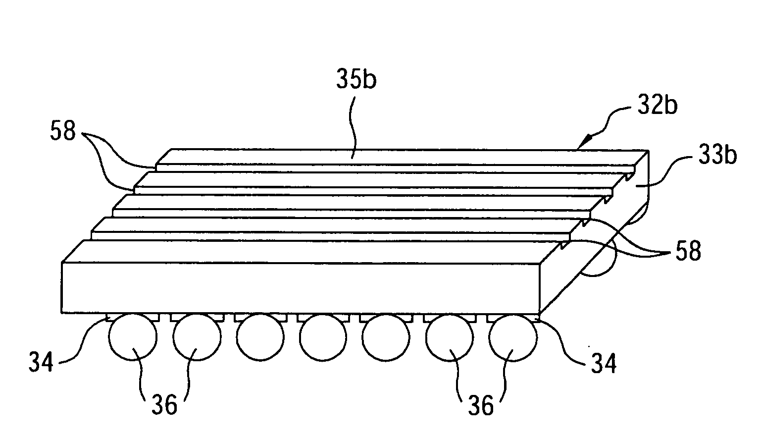
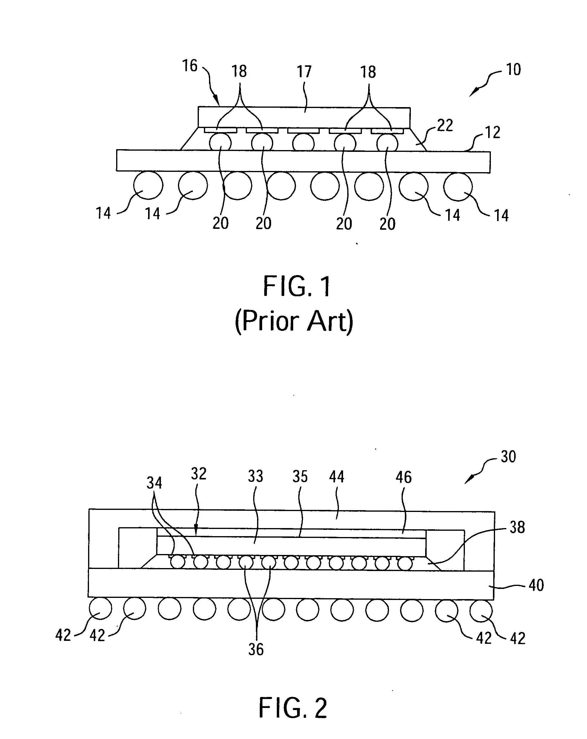
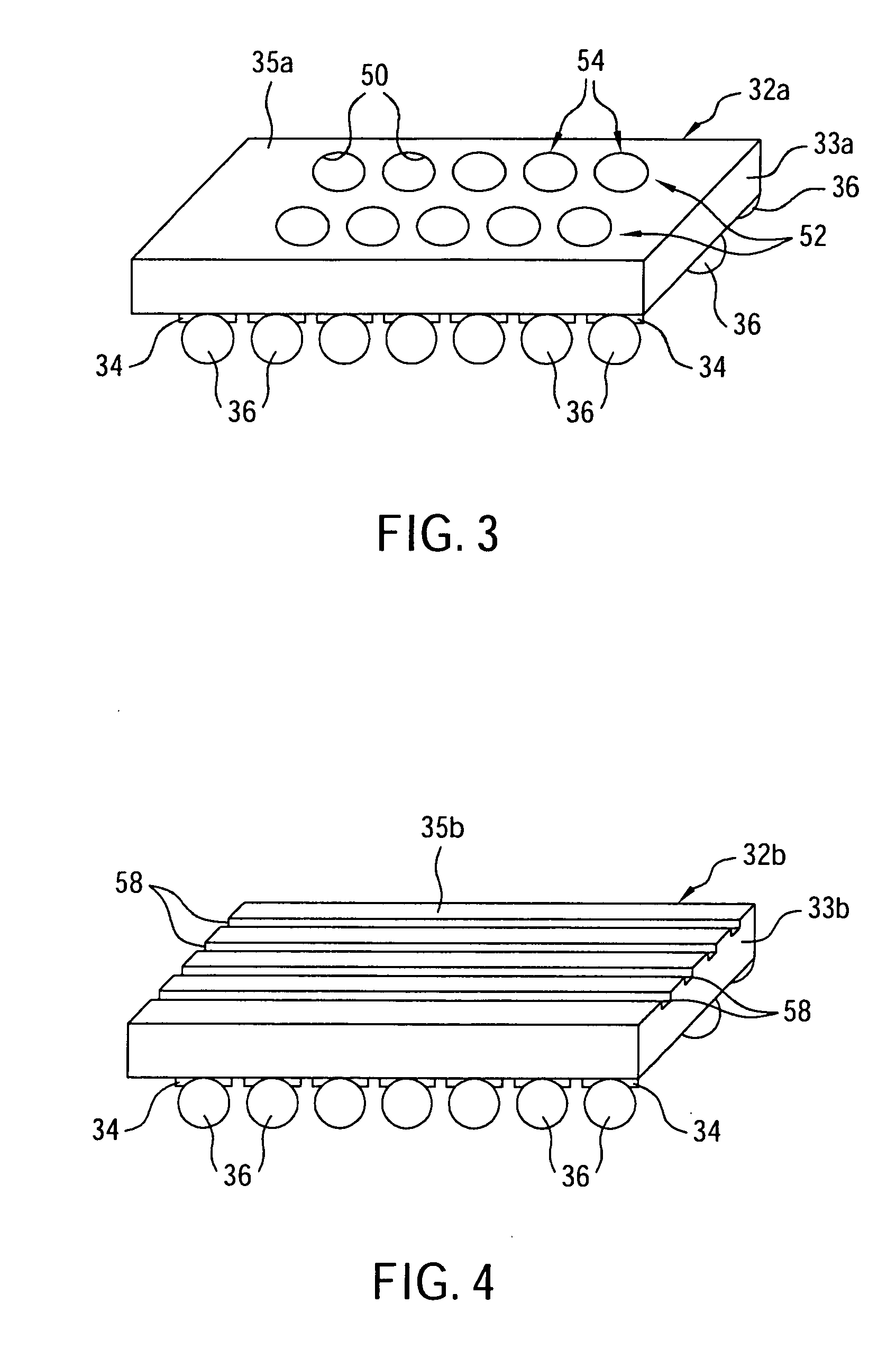
[0025] The present invention contemplates a novel IC chip package structure in which multiple solder bumps of an IC flip chip or die are bonded to a carrier substrate such as a printed circuit board (PCB). An adhesive material such as epoxy is sandwiched between the flip chip and the carrier substrate. According to the invention, concave stress-relieving structures are provided in the backside of the IC flip chip. In one embodiment, the stress-relieving structures are stress relief openings. In another embodiment, the stress-relieving structures are stress relief slots. In still another embodiment, the stress-relieving structures are stress-relief channels which are arranged in a symmetrical channel matrix. In yet another embodiment, the stress-relieving structures are stress-relief channels which arranged in an asymmetrical channel matrix. During thermal testing and / or functioning of the flip chip, the stress-relieving structures reduce stresses between the flip chip and the carrie...


PUM


Abstract

A novel chip packaging structure is disclosed. The chip packaging structure includes a flip chip having a chip backside, at least one concave stress-relieving structure provided in the chip backside, a carrier substrate bonded to the flip chip and an adhesive material interposed between the flip chip and the carrier substrate. During thermal testing and/or functioning of the flip chip, the stress-relieving structure reduces stresses between the flip chip and the carrier substrate and dissipates heat from the flip chip to reduce thermally-induced delamination stresses applied to the adhesive material and thereby enhances reliability of the flip chip.

Description

FIELD OF THE INVENTION [0001] The present invention relates to flip chip packaging of integrated circuit (IC) semiconductor assemblies. More particularly, the present invention relates to a novel IC chip package structure which utilizes openings, slots or a meshwork of channels to dissipate heat and enhance thermal transference efficiency between an IC (integrated circuit) device and a PCB (printed circuit board) substrate. BACKGROUND OF THE INVENTION [0002] One of the last processes in the production of semiconductor integrated circuits (IC) is multi-leveled packaging, which includes expanding the electrode pitch of the IC chips containing the circuits for subsequent levels of packaging; protecting the chip from mechanical and environmental stress; providing proper thermal paths for channeling heat dissipated by the chip; and forming electronic interconnections. The manner in which the IC chips are packaged dictates the overall cost, performance, and reliability of the packaged chi...

Claims


Application Information

Patent Timeline
IPC IPC(8): H01L21/00H01L29/06H01L23/34H01L23/48
CPCH01L23/367H01L23/42H01L2924/014H01L24/81H01L29/0657H01L2224/16H01L2224/73253H01L2224/8121H01L2224/81815H01L2924/01082H01L2924/10158H01L2924/14H01L2924/15311H01L2924/16152H01L2924/01006H01L2924/01033H01L2924/0105H01L2924/01075H01L2224/05573H01L2224/05568H01L2924/00014H01L2224/05599
Inventor CHEN, HSIEN-WEI
Owner TAIWAN SEMICON MFG CO LTD
Why Eureka
Try Eureka