

Electronic component and its manufacturing method
- Summary
- Abstract
- Description
- Claims
- Application Information
AI Technical Summary
Benefits of technology
Problems solved by technology
Method used
Image

Examples
first preferred embodiment
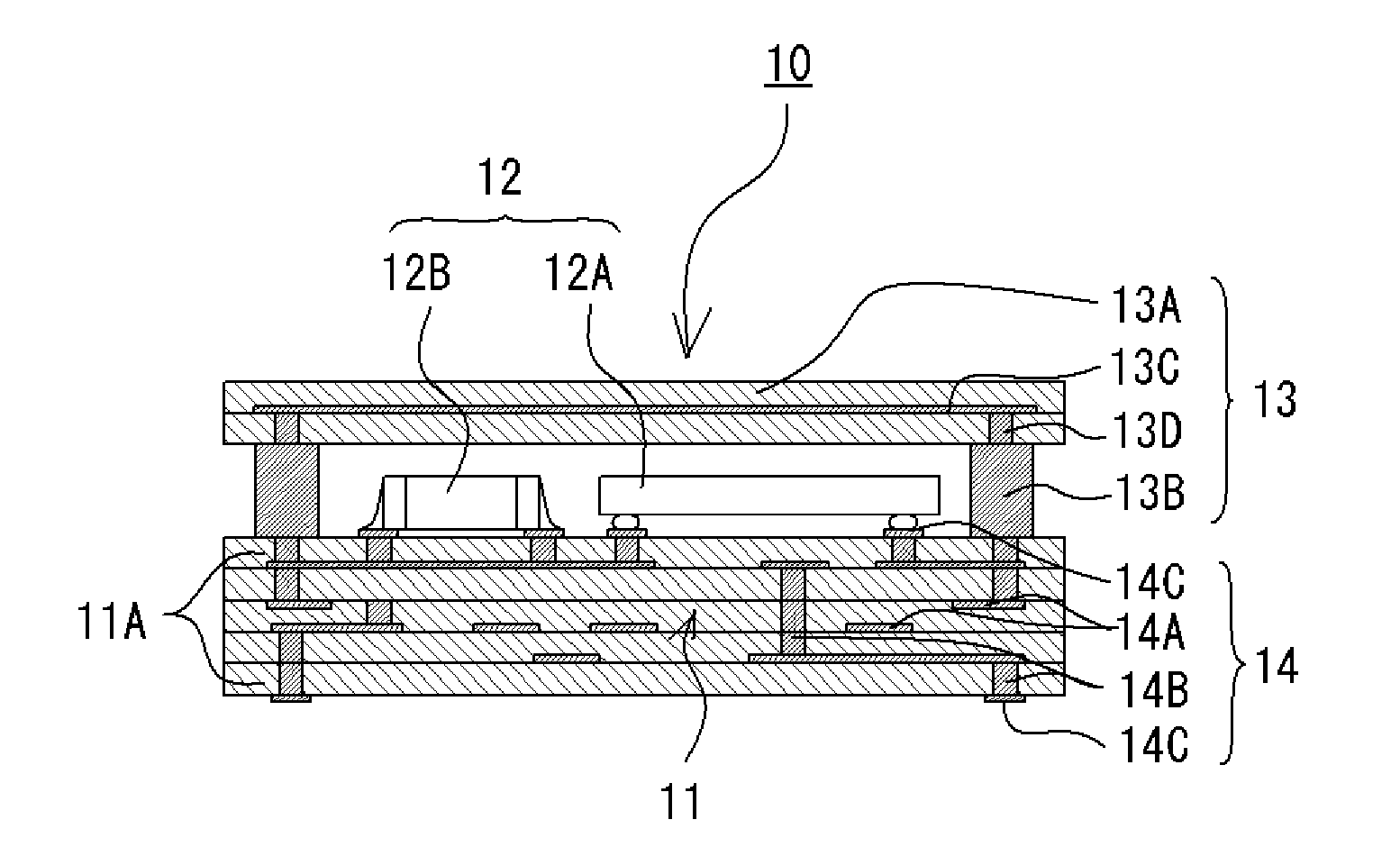
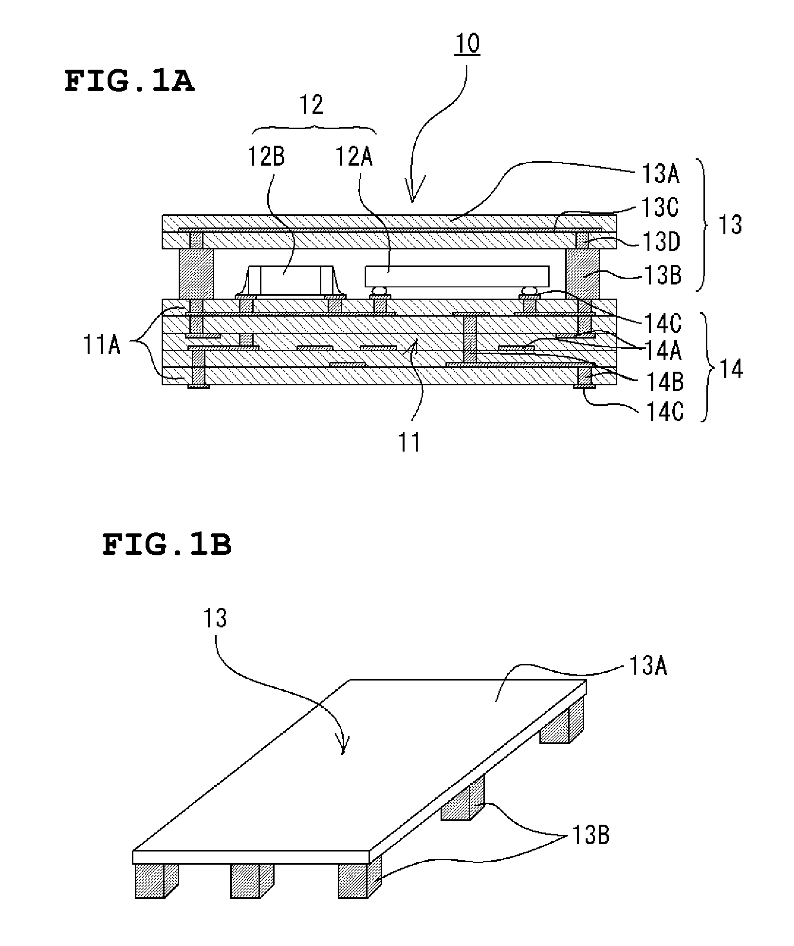
[0054] As shown in FIG. 1A, for instance, an electronic component 10 of the present preferred embodiment preferably includes a wiring board 11 having a predetermined wiring pattern, a plurality of surface mount devices 12 mounted on a main surface (an upper surface) of the wiring board, and a cover member 13 arranged to cover the surface mount devices 12. For example, the electronic component 10 is mounted on a mount board, such as a mother board (not shown).
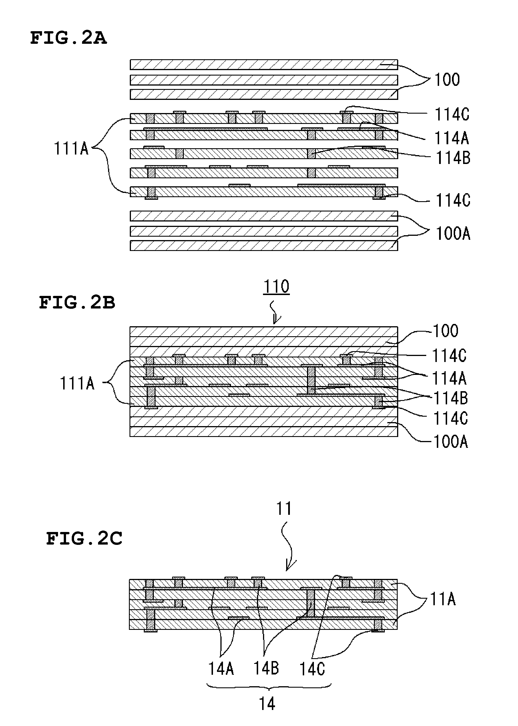
[0055] As shown in FIG. 1A, the wiring board 11 is, for example, a ceramic multilayered board in which a plurality of ceramic layers 11A are laminated. A wiring pattern 14 includes an in-plane conductor 14A having a predetermined pattern and arranged at an interface between vertically arranged ceramic layers 11A and 11A, a via conductor 14B having a predetermined pattern and penetrating through the ceramic layers 11A so as to electrically connect the vertically arranged in-plane conductors 14A and 14A, and surface electrodes (t...
second preferred embodiment
[0088] In an electronic component of this preferred embodiment, the same numerals refer the same portions as those of the first preferred embodiment or portions corresponding to those of the first preferred embodiment. The above preferred embodiment describes the electronic component 10 in which the shield electrode layer 13C of the cover member 13 covers all surface mount devices 12. Meanwhile, the surface mount devices 12 may include a surface mount device 12, such as a type of SAW filter package, of which a characteristic is varied in accordance with the distance with respect to the shield electrode layer 13C, which is the ground potential of the cover member 13. For example, if the top portion 13A of the cover member 13 is bent by a jig or other external force during the characteristic screening of the electronic component 10, the distance between the shield electrode layer 13C of the cover member 13 and the surface mount device 12 varies, and this may affect the characteristic ...
third preferred embodiment
[0091] An electronic component of this preferred embodiment is similar to that of the first preferred embodiment except that a leg portion 13B of a cover member 13 has a different shape as shown in FIG. 11A. The same numerals refer the same portions as those of the first preferred embodiment or portions corresponding to those of the first preferred embodiment.
[0092] While the above preferred embodiments have the leg portion 13B of the cover member 13 preferably having a uniform diameter as shown in FIG. 11B, the leg portion 13B of this preferred embodiment has a cross section along the shaft center with a tapered shape, namely, the leg portion 13B is formed in an inverted truncated cone shape, or an inverted quadrangular pyramid shape, as shown in FIG. 11A. The leg portion 13B is formed such that a via hole is provided at the shrinkage-suppression sheet so as to have a tapered cross section, and the via hole is filled with the conductive paste. The leg portion 13B having the cross ...
PUM
| Property | Measurement | Unit |
|---|---|---|
| Temperature | aaaaa | aaaaa |
| Height | aaaaa | aaaaa |
Abstract
Description
Claims
Application Information