Eureka AIR delivers breakthrough ideas for toughest innovation challenges, trusted by R&D personnel around the world.

Method of monitoring a semiconductor processing system using a wireless sensor network

Active Publication Date: 2007-09-27
TOKYO ELECTRON LTD
View PDF51 Cites 38 Cited by
  • Summary
  • Abstract
  • Description
  • Claims
  • Application Information

AI Technical Summary

Benefits of technology

[0009] The semiconductor processing system includes a plurality of system components configured to flow a process gas through the semiconductor processing system, and a wireless sensor network comprising a plurality of non-invasive sensors positioned on respective outer surfaces of one or more of the plurality of system components. The sensors are configured for

Problems solved by technology

Changes in processing conditions of a processing (manufacturing) system employed in semiconductor manufacturing can lead to significant loss of revenue due to scrap and non-productive system downtime.
In this regard, focus has been placed on system software that monitors operation of the manufacturing system and creates alarms when unacceptable process excursions occur or other fault conditions are encountered.
However, the method of using scheduled preventive maintenance is simply based on “rules of thumb” derived from average characteristics, such as mean time between failures (MTBF), and does not address detection, diagnosis, or prediction of faulty conditions for individual processing system components or entire processing systems.
In addition, this method does not address gradual degradation or drift in the processing conditions of the processing system.
Traditionally, the cost and bulk of sensing technology means that only a handful of hardwired sensors with little flexibility and networking capability could be deployed for most processing systems.
The information collected from the few sensors only provides a relatively small amount of data and does not provide desired real-time monitoring and analysis capabilities needed for comprehensive understanding of the processing condition of the processing system.

Method used


Image

  • Method of monitoring a semiconductor processing system using a wireless sensor network
  • Method of monitoring a semiconductor processing system using a wireless sensor network
  • Method of monitoring a semiconductor processing system using a wireless sensor network

Examples


example

Vibrational Signature of a Gas Line During Process Gas Flow

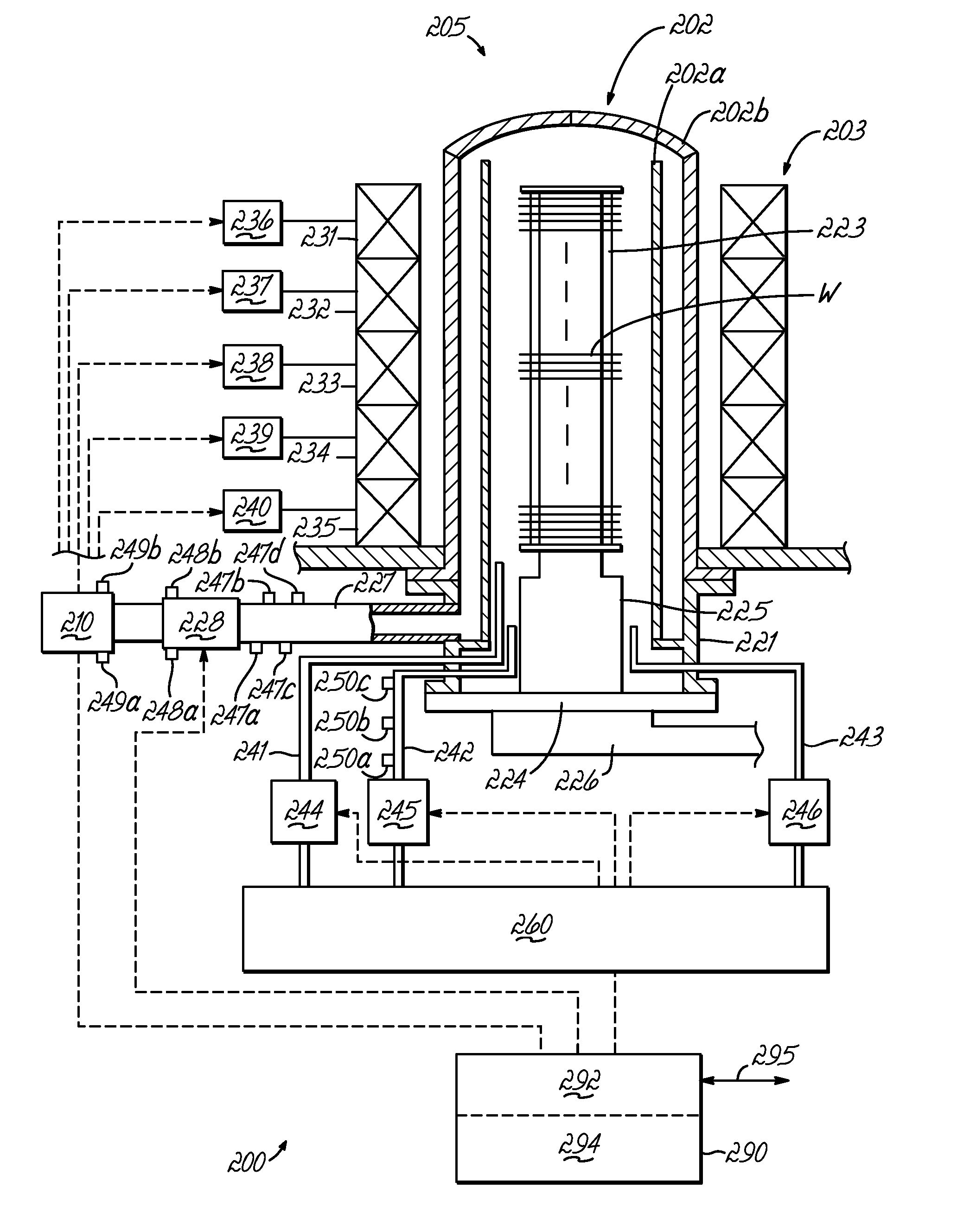
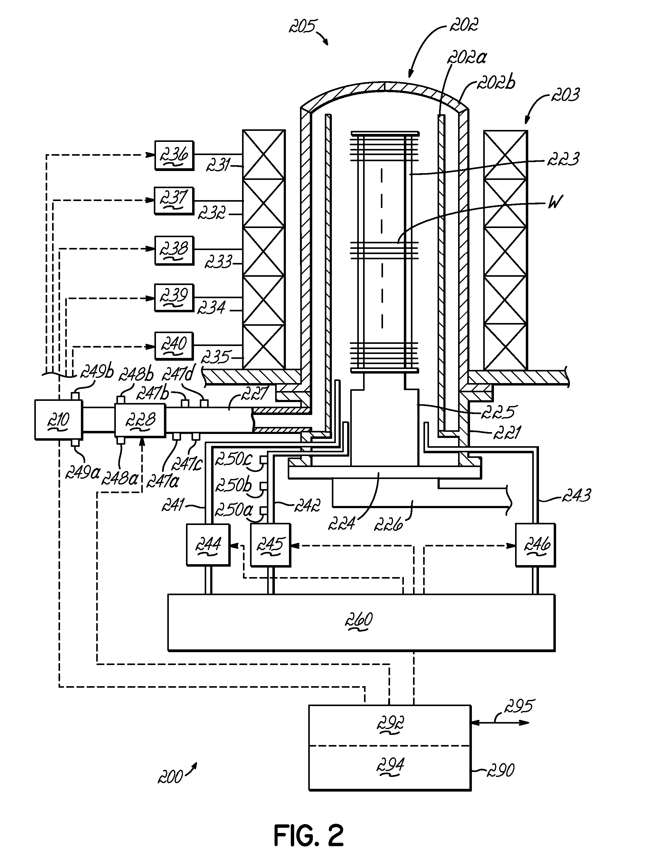
[0085] Under certain flow conditions, flow of a process gas through gas lines found in semiconductor manufacturing systems (e.g., thermal processing system 200 in FIG. 2), can develop high levels of noise and vibrations. For example, process gas flow through gas supply line 242 or gas exhaust line 227, can excite a standing wave, resulting in vibrations in the gas line that can be greatly amplified if acoustic or structure resonance occurs. A clean gas line may produce a baseline vibrational signature as a process gas flows through the system component, and changes in the vibrational signature of the gas line can indicate a change in the dynamic characteristics of the gas line (e.g., formation of a material deposit in the gas line) and the overall processing system. The changes may be analyzed and compared to a baseline vibrational signature in order to diagnose a drift or a failure in the processing system so that appropri...


PUM


Abstract

A method and system for non-invasive sensing and monitoring of a processing system employed in semiconductor manufacturing. The method allows for detecting and diagnosing drift and failures in the processing system and taking the appropriate correcting measures. The method includes positioning at least one non-invasive sensor on an outer surface of a system component of the processing system, where the at least one invasive sensor forms a wireless sensor network, acquiring a sensor signal from the at least one non-invasive sensor, where the sensor signal tracks a gradual or abrupt change in a processing state of the system component during flow of a process gas in contact with the system component, and extracting the sensor signal from the wireless sensor network to store and process the sensor signal. In one embodiment, the non-invasive sensor can be an accelerometer sensor and the wireless sensor network can be motes-based.

Description

CROSS REFERENCE TO RELATED APPLICATION [0001] This application is related to co-pending U.S. patent application Ser. No. ______, filed on even date herewith and entitled “Semiconductor Processing System With a Wireless Sensor Network Monitoring System Incorporated Therewith,” the disclosure of which is incorporated herein by reference in its entirety as if completely set forth herein below.FIELD OF THE INVENTION [0002] Embodiments of the invention relate generally to a monitoring system and method for non-invasive sensing and monitoring of a processing system employed in semiconductor manufacturing. The method and system allow for detecting and diagnosing drift and failures in the processing system and taking the appropriate correcting measures. BACKGROUND OF THE INVENTION [0003] Changes in processing conditions of a processing (manufacturing) system employed in semiconductor manufacturing can lead to significant loss of revenue due to scrap and non-productive system downtime. In th...

Claims


Application Information

Patent Timeline
IPC IPC(8): H01L21/66H01L21/00G01R31/26
CPCH01L21/67253
Inventor KAUSHAL, SANJEEVSUGISHIMA, KENJIRAO, DONTHINENI RAMESH KUMAR
Owner TOKYO ELECTRON LTD
Why Eureka
Eureka Blog
Learn More