

Heat treatment apparatus of light emission type
a technology of heat treatment apparatus and light emission, which is applied in the field of heat treatment apparatus, can solve the problems of imposing an enormous operation load, complicated operation, and apprehension of a hindrance to good device formation, and achieves the effect of high durability
- Summary
- Abstract
- Description
- Claims
- Application Information
AI Technical Summary
Benefits of technology
Problems solved by technology
Method used
Image

Examples
Embodiment Construction
[0026]The preferred embodiments of the present invention will now be discussed in detail with reference to the drawings.
1. The First Preferred Embodiment
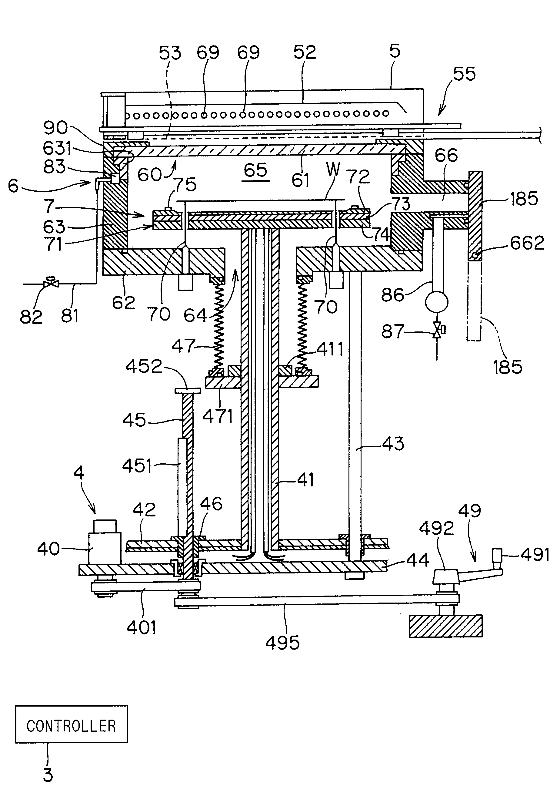
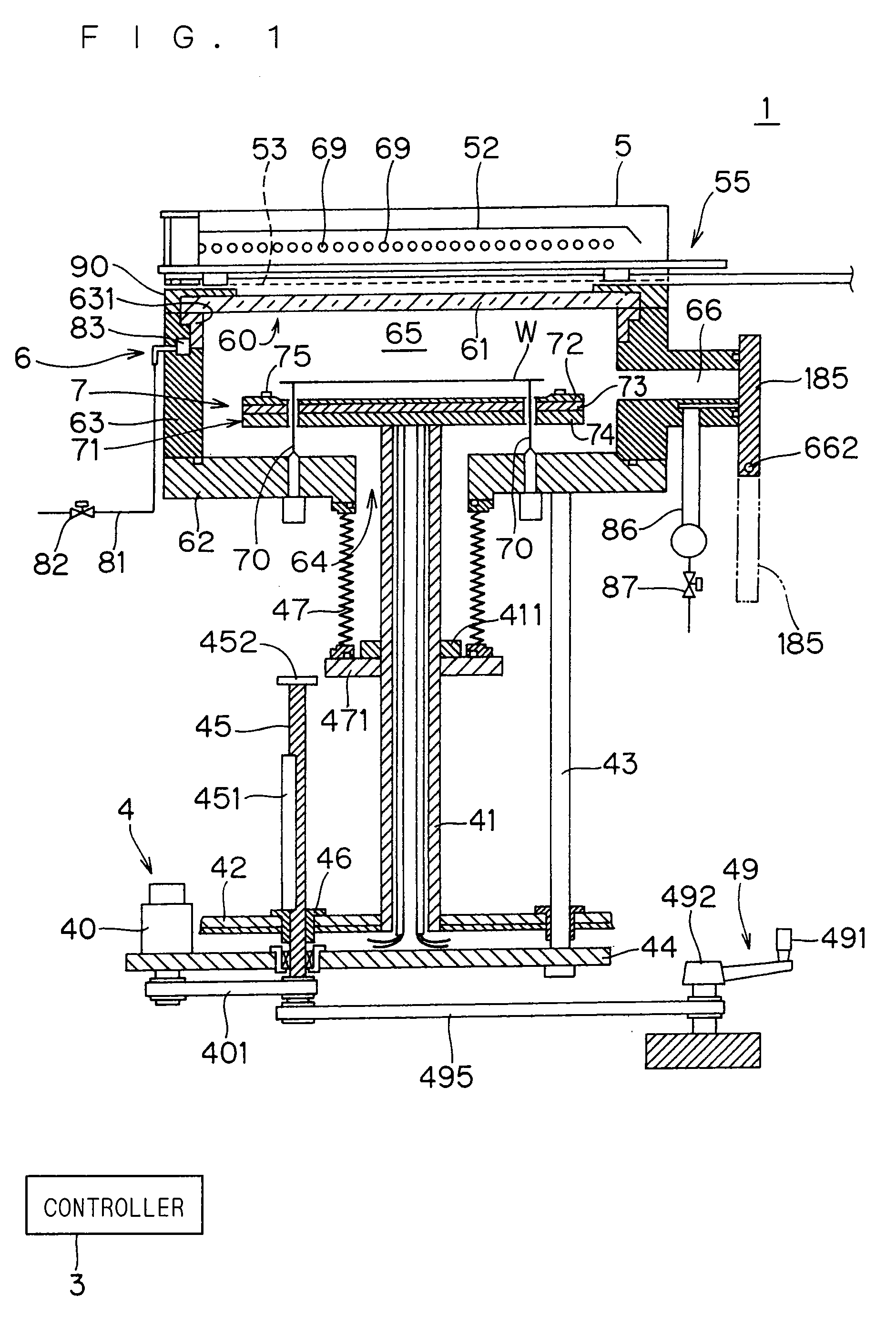
[0027]First, the overall construction of a heat treatment apparatus in accordance with the present invention will be outlined. FIG. 1 is a sectional side view showing the construction of a heat treatment apparatus 1 in accordance with the present invention. The heat treatment apparatus 1 is a flash lamp annealer for exposing a semiconductor wafer W of generally circular shape, serving as a substrate, to a flash of light to heat the semiconductor wafer W.
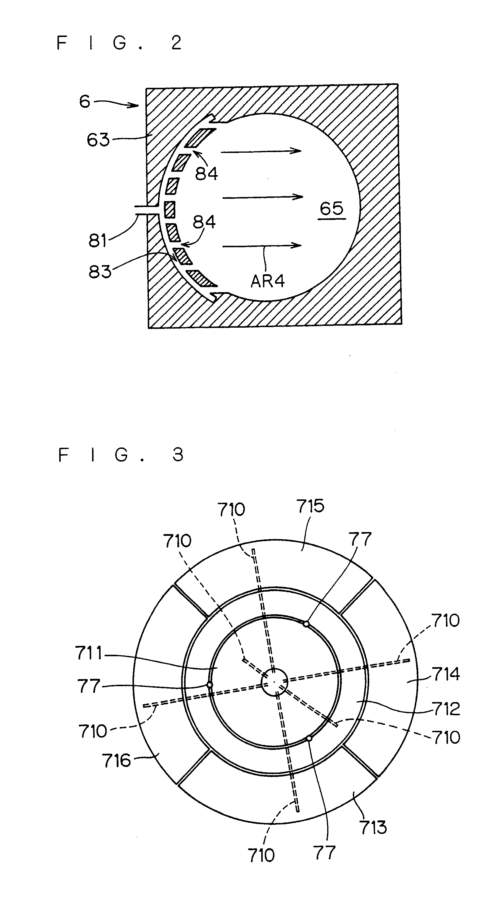
[0028]The heat treatment apparatus 1 comprises a chamber 6 of generally cylindrical configuration for accommodating a semiconductor wafer W therein. The chamber 6 includes a chamber side portion 63 having an inner wall of generally cylindrical configuration, and a chamber bottom portion 62 for covering a bottom portion of the chamber side portion 63. A space surrounded by the chamber...
PUM
| Property | Measurement | Unit |
|---|---|---|
| Electric potential / voltage | aaaaa | aaaaa |
Abstract
Description
Claims
Application Information