Transmitter voltage and receiver time margining

a technology of transceiver voltage and receiver time, applied in the field of integrated circuits, can solve the problems of difficult measurement, inability to provide useful information with respect to signal characteristics at the integrated circuit pad, and difficulty in quantifying the operating margin of a particular data communication system

Active Publication Date: 2007-10-04
ADVANCED MICRO DEVICES INC
View PDF57 Cites 35 Cited by
  • Summary
  • Abstract
  • Description
  • Claims
  • Application Information

AI Technical Summary

Problems solved by technology

System level characterization at pins of an integrated circuit in a data communications system operating at high frequency rates (e.g., 1.0 GHz or greater) may be difficult to measure and may not provide useful information with respect to signal characteristics at the integrated circuit pad.
Therefore, it is difficult to quantify the operating margin of a particular data communications system.
Probing signals at the integrated circuit pad may ...

Method used


Image

  • Transmitter voltage and receiver time margining
  • Transmitter voltage and receiver time margining
  • Transmitter voltage and receiver time margining

Examples


Embodiment Construction

)

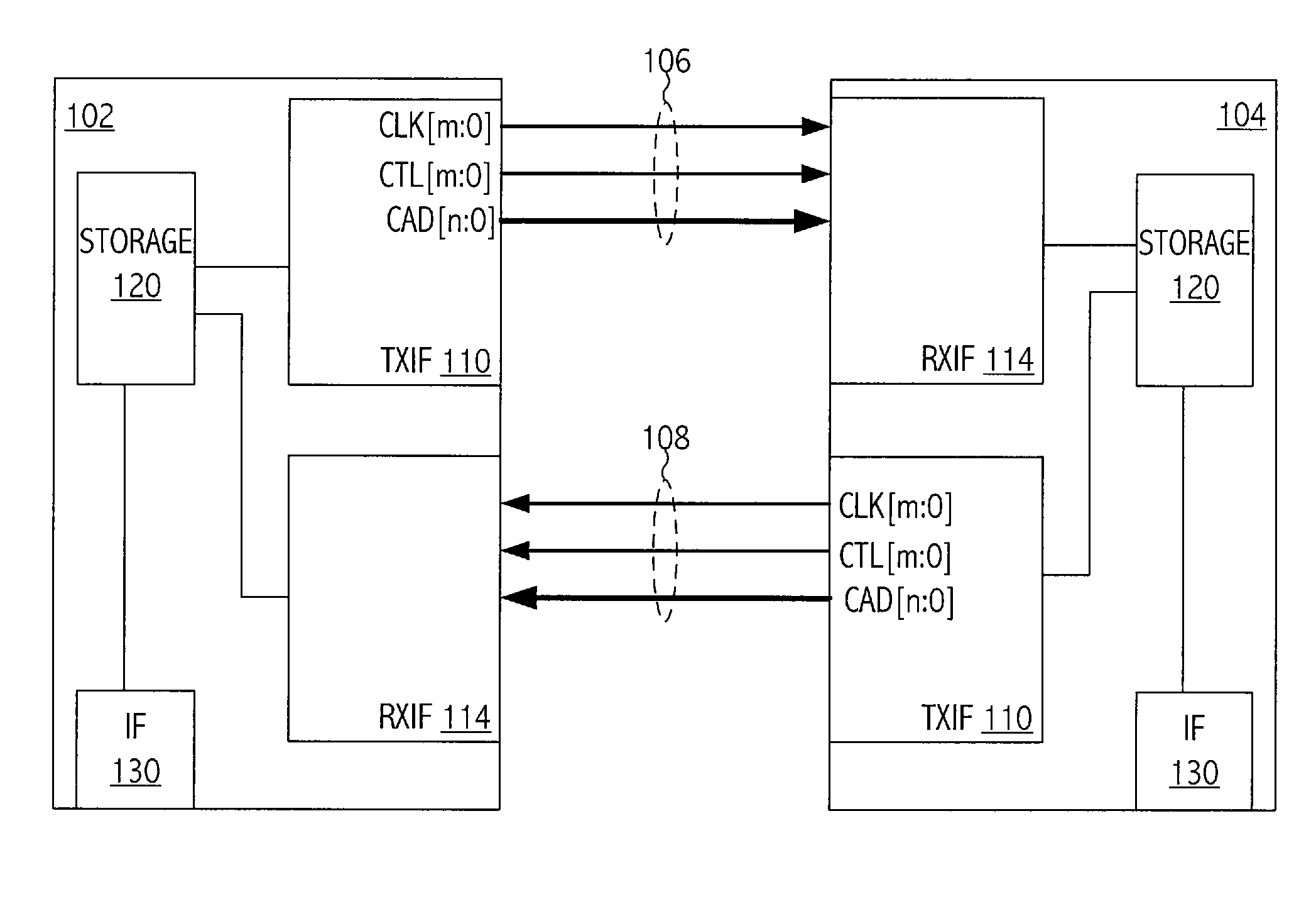
[0023]Referring to FIG. 1, integrated circuit 102 communicates with integrated circuit 104 by an exemplary communications link including transmit interfaces 110, receive interfaces 114, and communications paths 106 and 108, which include respective, individual communications paths for clock signals (e.g., CLK[m:0]), control signals (e.g., CTL[m:0]), and data signals (e.g., n-bits of commands, addresses, or data, i.e., CAD[n:0]). Those individual communications paths may be single-ended or differential communications paths. In at least one embodiment of the communications link, a bit-time is half a clock period in duration, i.e., two data bits (e.g., two CAD[n:0] bits or two CTL[m:0] bits) are transmitted on a corresponding communications path per clock cycle (e.g., a period of a respective one of CLK[m:0]). However, the teachings herein may be adapted for bit-times having one clock period in duration (i.e., one data bit is transmitted on a corresponding communications path per cloc...


PUM


Abstract

A technique for characterizing a communications interface includes determining a voltage margin and a timing margin of the interface based on data sampled by a sampling device of a receiver of the interface. In at least one embodiment of the invention, a method for determining margin associated with a receiver circuit of an integrated circuit includes periodically sampling a signal over a time period by a receiver sampling circuit of the receiver circuit to generate a sampled version of the signal. The method includes incrementally varying a value of the parameter associated with the signal. The varying of the parameter is through a range of values of the parameter over the time period. The method includes determining a margin value of the receiver circuit associated with the parameter based, at least in part, on the sampled version of the signal.

Description

CROSS-REFERENCE TO RELATED APPLICATION(S)[0001]This application claims benefit under 35 U.S.C. § 119 of provisional application No. 60 / 786,546, filed Mar. 28, 2006, entitled “Method and Apparatus for Link Operations,” naming Gerry R. Talbot, Paul Miranda, Mark D. Hummel, William A. Hughes, and Larry D. Hewitt as inventors, which application is incorporated by reference herein.BACKGROUND[0002]1. Field of the Invention[0003]This application is related to integrated circuits and more particularly to data communications links between integrated circuits.[0004]2. Description of the Related Art[0005]System level characterization at pins of an integrated circuit in a data communications system operating at high frequency rates (e.g., 1.0 GHz or greater) may be difficult to measure and may not provide useful information with respect to signal characteristics at the integrated circuit pad. Therefore, it is difficult to quantify the operating margin of a particular data communications system....

Claims


Application Information

Patent Timeline
IPC IPC(8): H04J3/06
CPCH04L7/0337G01R31/30H04L1/20G01R31/316G01R31/317G01R31/3004
Inventor TALBOT, GERALD R.MIRANDA, PAUL C.FANG, EMERSON S.KUMAR, ROHIT
Owner ADVANCED MICRO DEVICES INC
Why Eureka
Try Eureka