Semiconductor device and method for manufacturing the same

Inactive Publication Date: 2007-10-04
FUJITSU LTD
View PDF3 Cites 14 Cited by
  • Summary
  • Abstract
  • Description
  • Claims
  • Application Information

AI Technical Summary

Benefits of technology

[0015]The semiconductor device has the first conductive layer and the second conductive layer. For this reason, it exhibits greater strength on the conductive layer side during packaging through external terminals such as bumps as compared to the conventional semiconductor device with only one conductive layer, allows diffusion of stress due to thermal stress and suppresses peeling off of conductive layer as well as peeling off of interconnection layer by inhibiting stress on the interconnection layer side. Therefore, the semiconductor device of the present invention is of high performance and reliability and particularly suitable for wafer-level package.
[0017]In the method for manufacturing the semiconductor device, the interconnection layer is formed over the semiconductor substrate in the forming step of interconnection layer. The first conductive layer is formed over the interconnection layer in the forming step of first conductive layer. The interlayer insulating film is formed over the first conductive layer in the forming step of interlayer insulating film. The second conductive layer is formed over the interlayer insulating film in the forming step of second conductive layer. As a result, a number of the conductive layers are formed and the strength on the conductive layer becomes greater during packaging through external terminals such as bumps, allowing diffusion of stress due to thermal stress and suppressing peeling off of conductive layer as well as peeling off of interconnection layer by inhibiting stress on the interconnection layer side. Therefore, semiconductor devices with high performance and reliability are manufactured efficiently.

Problems solved by technology

Meanwhile, high pin-count and miniaturization of the semiconductor device resulted from the increase in density leads to narrow pitches between adjacent external terminals.
However, there is a problem that the multilayered interconnection of interconnection layers or conductive layer (electrode pads) is likely to be peeled off by stress on the semiconductor chip side due to thermal stress generated from the thermal contraction of the opposite substrate, which is greater as compared to that of the semiconductor chip.
Moreover, because a lead-free material with a high degree of hardness is used for bumps, plastic deformation capacity is low, allowing greater stress on the semiconductor chip side, thereby causing peeling off of interconnection layers and conductive layers.
Therefore, semiconductor devices with high performance and reliability, in which peeling off of interconnection layers or conductive layers due to thermal stress developed during packaging is suppressed, and methods for manufacturing the semiconductor devices have not yet been provided.

Method used


Image

  • Semiconductor device and method for manufacturing the same
  • Semiconductor device and method for manufacturing the same
  • Semiconductor device and method for manufacturing the same

Examples


example 1

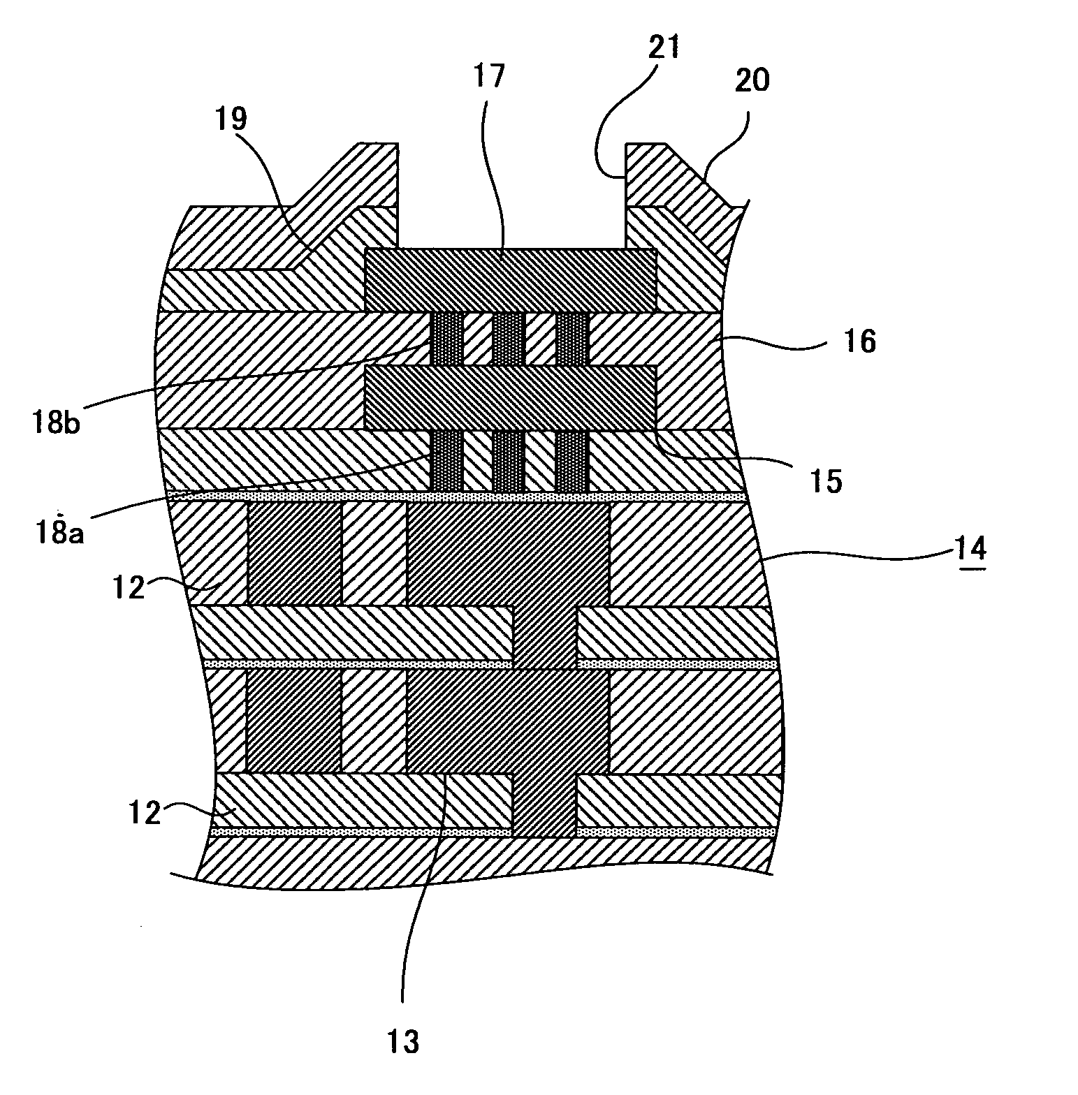
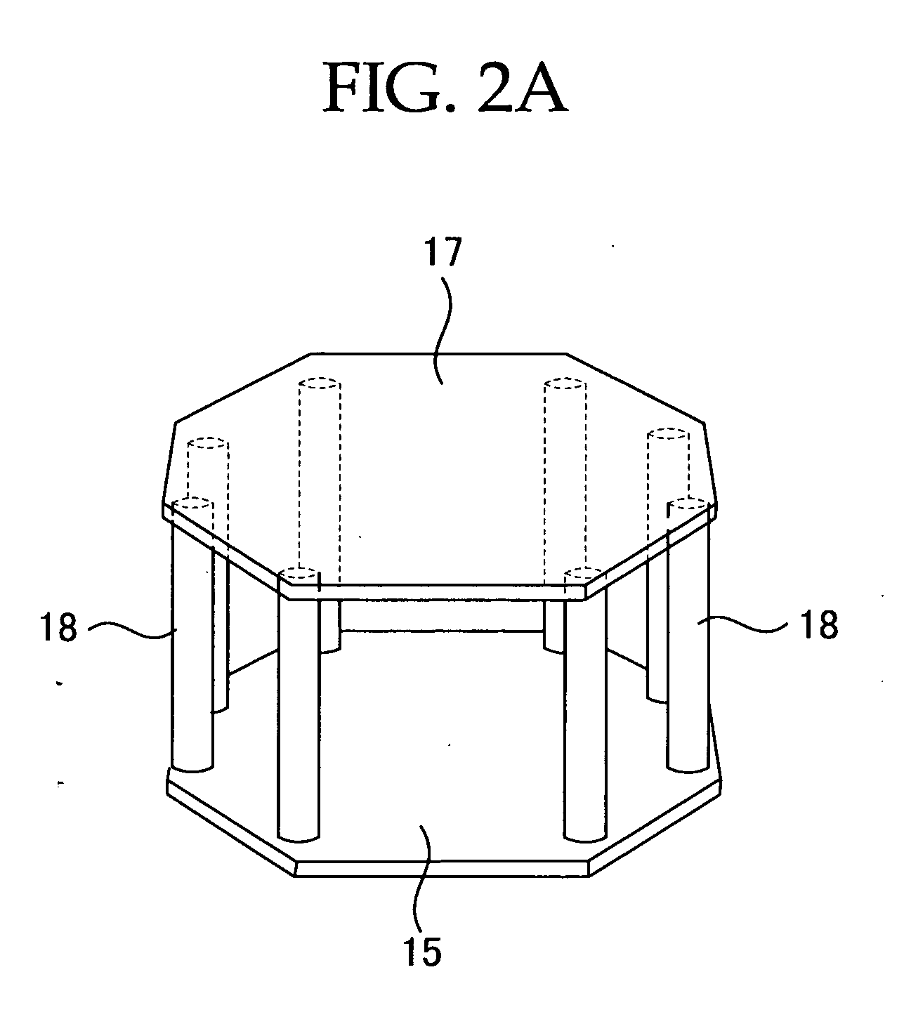
[0054]The First Example of the semiconductor device of the present invention is shown in FIG. 1. In the semiconductor device as shown in FIG. 1, an interlayer insulating film 12 made of, for example, polyimide resin and an interconnection layer 14 made of a multilayered interconnection 13 are formed over a silicon wafer 10 which serves as the foregoing semiconductor substrate. A first conductive layer 15 made of Al pad is formed over the interconnection layer 14 and an interlayer insulating film 16 made of polyimide resin and / or epoxy resin, etc. is formed over the first conductive layer 15. A second conductive layer 17 made of Al pad is formed over the interlayer insulating film 16. The second conductive layer 17 and the first conductive layer 15 are electrically connected by a number of vias 18 which are vertically disposed in the vicinity of an outer periphery of the first and the second conductive layers 15 and 17. Moreover, the vicinity of an outer periphery of the second condu...

example 2

[0084]Hereinafter, an exemplary method for manufacturing the semiconductor device of the present invention of Example 2 will be explained referring to figures. The wafer-level packaging technology may be used for the manufacture of the semiconductor device of Example 2.

[0085]First, as shown in FIG. 13, an interconnection layer 14 containing an interlayer insulating film 12 and a multilayered interconnection 13 was formed over a silicon wafer 10 as the semiconductor substrate by the general manufacturing process for wafer as similar to Example 1. A first conductive layer 15 was formed over the interconnection layer 14 and a first resin film 19 made of SiO2 and a second resin film 20 made of polyimide resin were formed over the first conductive layer 15 in this order. An opening 21 was formed in the first and the second resin films 19 and 20 by etching to expose a surface of the first conductive layer 15 from the opening 21.

[0086]The forming steps of the second conductive layer, etc. ...


PUM


Abstract

It is an object of the present invention to provide a semiconductor device with high performance and reliability, in which peeling off of interconnection layers or conductive layers due to thermal stress developed during packaging of a semiconductor substrate is suppressed, and thus electrical break down is prevented and an efficient method for manufacturing the semiconductor device. The semiconductor device of the present invention is characterized by having a semiconductor substrate, an interconnection layer 12, a first conductive layer 15, an interlayer insulating film 16 and a second conductive layer 17. The method for manufacturing the semiconductor device of the present invention is characterized by containing at least forming an interconnection layer, forming a first conductive layer, forming an interlayer insulating film and forming a second conductive layer so as to be electrically connected to the first conductive layer.

Description

CROSS-REFERENCE TO RELATED APPLICATIONS[0001]This application is based upon and claims the benefits of the priority from the prior Japanese Patent Application No. 2006-095737, filed on Mar. 30, 2006, the entire contents of which are incorporated herein by reference.BACKGROUND OF THE INVENTION[0002]1. Field of the Invention[0003]The present invention relates to a semiconductor device with high performance and reliability, in which peeling off of interconnection layers or conductive layers due to thermal stress developed during packaging of a semiconductor substrate is suppressed, and thus electrical break down is prevented, and an efficient method for manufacturing the semiconductor device.[0004]2. Description of the Related Art[0005]Attempts have been made in recent years to achieve downsizing and greater packaging density of semiconductor devices, with the trend moving toward for thinner, smaller electronic devices. Against this background, wafer level packaging has been proposed, ...

Claims


Application Information

Patent Timeline
IPC IPC(8): H01L21/4763
CPCH01L21/768H01L2924/0002H01L2224/0401H01L2224/02166H01L2924/01075H01L2924/01074H01L2924/01006H01L2924/3025H01L23/293H01L23/3192H01L24/03H01L24/05H01L24/13H01L2224/0345H01L2224/03912H01L2224/05012H01L2224/05086H01L2224/05095H01L2224/05124H01L2224/05571H01L2224/05573H01L2224/05666H01L2224/1146H01L2224/1147H01L2224/11849H01L2224/131H01L2924/01013H01L2924/01029H01L2924/01033H01L2924/01078H01L2924/01082H01L2924/014H01L2924/00014H01L2224/05552H01L2924/351H01L2924/15787H01L2924/01014H01L2924/00
Inventor SAITOU, NOBUKATSUUNO, TADASHIKANO, MASASHIMATSUOKA, YOSHIHIRO
Owner FUJITSU LTD
Why Eureka
Try Eureka