Substrate holding apparatus, polishing apparatus, and polishing method

a technology of holding apparatus and substrate, which is applied in the direction of grinding drive, grinding machine, manufacturing tools, etc., can solve the problems of short circuit, large step height on the surface of semiconductor devices, complicated structure of semiconductor elements, etc., and achieve the effect of stably polishing substra

Active Publication Date: 2007-10-04
EBARA CORP
View PDF59 Cites 30 Cited by
  • Summary
  • Abstract
  • Description
  • Claims
  • Application Information

AI Technical Summary

Benefits of technology

[0011]The present invention has been made in view of the above situation in the related art. It is therefore an object of the present invention to provide a substrate holding apparatus, a polishing apparatus, and a polishing method which are effective to prevent a substrate as a workpiece to be polished from being slipping out and to allow the substrate to be polished stably.
[0012]According to a first aspect of the present invention, there is provided a substrate holding apparatus which prevents a substrate as a workpiece to be polished from slipping out and allows the substrate to be polished stably. The substrate holding apparatus comprises a top ring body for holding and pressing a substrate against a polishing surface, and a retainer ring for pressing the polishing surface, the retainer ring being disposed on an outer circumferential portion of the top ring body. The retainer ring comprises a first member made of a magnetic material and a second member having a magnet disposed on a surface thereof which is held in abutment against the first member.
[0013]Since the first member and the second member of the retainer ring are thus secured to each other under magnetic forces, the first member and the second member remain to stick together even when the retainer ring is vibrated during the polishing process. The retainer ring is prevented from being abruptly lifted off the polishing surface due to vibration. Therefore, the surface pressure imposed by the retainer ring is stabilized, reducing the possibility that the semiconductor wafer may slip out of the substrate holding apparatus. If a need arises to separate the first member and the second member from each other for maintenance or the like, then the coupling between the first member and the second member under magnetic forces is weakened to allow the first member and the second member to be separated easily from each other.
[0016]The heights of the retainer ring in at least two positions are detected by the sensors, and the gradient of the retainer ring is calculated from the detected heights by the processor. By thus calculating the gradient of the retainer ring, the processor can predict the possibility that the substrate held by the top ring body may slip out of the top ring body due to excessive inclination of the retainer ring. Therefore, the substrate can be prevented from slipping out of the top ring body based on the predicted possibility.
[0017]According to a third aspect of the present invention, there is provided a polishing method for stably polishing a substrate as a workpiece to be polished while preventing the substrate from slipping out. The polishing method polishes the substrate by holding an outer circumferential portion of the substrate with a retainer ring disposed on an outer circumferential portion of a top ring body, and pressing the substrate against a polishing surface with the top ring body while pressing the retainer ring against the polishing surface. The polishing method comprises measuring the gradient of the retainer ring, and generating an external alarm signal, stopping polishing the substrate, or changing to a preset polishing condition if the gradient of the retainer ring exceeds a predetermined threshold.

Problems solved by technology

In recent years, semiconductor devices have become more integrated, and structures of semiconductor elements have become more complicated.
Accordingly, irregularities on a surface of a semiconductor device become increased, so that step heights on the surface of the semiconductor device tend to be larger.
When irregularities of a surface of a semiconductor device are increased, the following problems arise: A thickness of a film formed in a portion having a step is relatively small when a thin film is formed on a semiconductor device.
An open circuit is caused by disconnection of interconnects, or a short circuit is caused by insufficient insulation between interconnect layers.
As a result, good products cannot be obtained, and yield tends to be reduced.
Further, even if a semiconductor device initially works normally, reliability of the semiconductor device is lowered after long-term use.
Therefore, if the irregularities on the surface of the semiconductor device are increased, then this becomes problematic in that it is difficult to form a fine pattern itself on the semiconductor device.
In such a polishing apparatus, if a relative pressing force between the semiconductor wafer being polished and the polishing surface of the polishing pad is not uniform over an entire surface of the semiconductor wafer, then the semiconductor wafer may insufficiently be polished or may excessively be polished at some portions depending on a pressing force applied to those portions of the semiconductor wafer.
Further, the polishing pad is so elastic that pressing forces applied to a peripheral portion of the semiconductor wafer being polished become non-uniform, and hence only the peripheral portion of the semiconductor wafer may excessively be polished, which is referred to as “edge rounding”.
However, the use of the retainer ring is problematic in that the semiconductor wafer held in place by the retainer ring tends to be accidentally dislodged from the substrate holding apparatus during the polishing process, and cannot stably be polished.

Method used


Image

  • Substrate holding apparatus, polishing apparatus, and polishing method
  • Substrate holding apparatus, polishing apparatus, and polishing method
  • Substrate holding apparatus, polishing apparatus, and polishing method

Examples


first embodiment

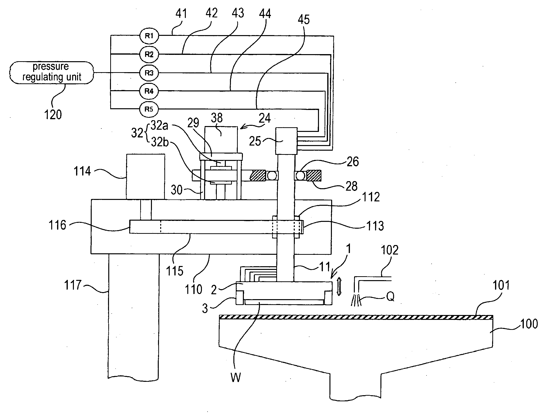
[0026]Embodiments of a substrate holding apparatus and a polishing apparatus according to the present invention will be described in detail below with reference to the drawings. FIG. 1 shows in schematic side view of a polishing apparatus incorporating a substrate holding apparatus according to the present invention. The substrate holding apparatus serves to hold a substrate, such as a semiconductor wafer or the like, as a workpiece to be polished and press the substrate against a polishing surface on a polishing table. As shown in FIG. 1, the polishing apparatus includes a top ring 1, which constitutes a substrate holding apparatus according to the present invention, and a polishing table 100 disposed below the top ring 1, with a polishing pad 101 attached to an upper surface of the polishing table 100. A polishing liquid supply nozzle 102 is disposed above the polishing table 100. The polishing liquid supply nozzle 102 supplies a polishing liquid Q onto the polishing pad 101 on th...

second embodiment

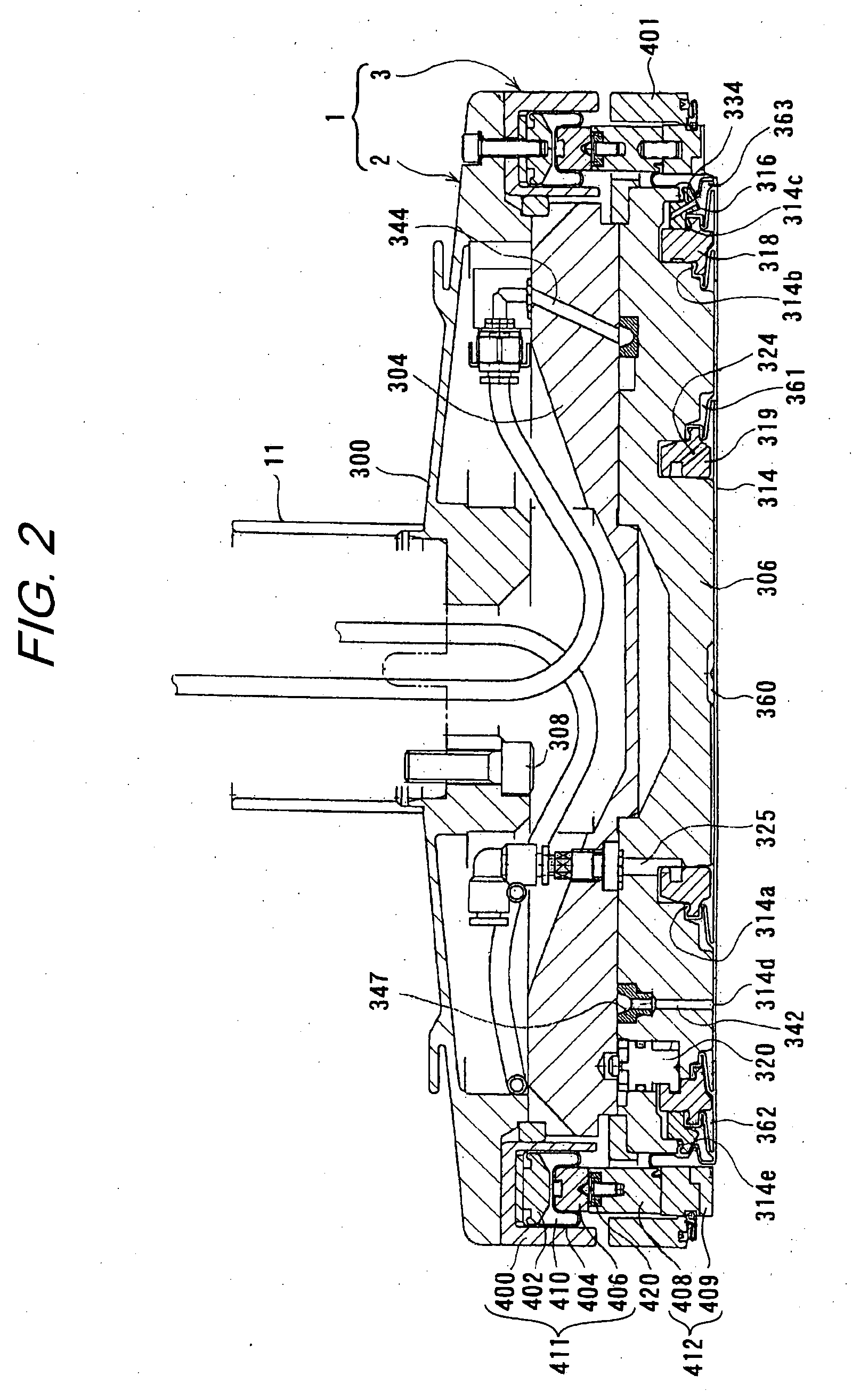
[0055]FIG. 5 shows in vertical cross section a substrate holding apparatus (top ring) 501 in a polishing apparatus according to the present invention. FIG. 6 shows in plan the polishing apparatus. Those parts of the top ring 501 which are identical to those shown in FIGS. 2 and 3 are denoted by identical reference characters, and will not be described in detail below. As shown in FIGS. 5 and 6, the top ring 501 of this embodiment has a ring-shaped measurement plate 502 mounted on an outer circumferential surface of the retainer ring portion 412 of the retainer ring 3. The top ring head, which serves as a mount on which the top ring 501 is mounted, has displacement sensors 506 disposed in respective two positions along the circumferential direction of the top ring 501. Each of the displacement sensors 506 has a roller 504 on its lower end. The displacement sensors 506 are electrically connected to a processor 508 for calculating the gradient of the retainer ring body 409 of the retai...


PUM


Abstract

A substrate holding apparatus prevents a substrate from slipping out and allows the substrate to be polished stably. The substrate holding apparatus has a top ring body for holding and pressing a substrate against a polishing surface, and a retainer ring for pressing the polishing surface, the retainer ring being disposed on an outer circumferential portion of the top ring body. The retainer ring comprises a first member made of a magnetic material and a second member having a magnet disposed on a surface thereof which is held in abutment against the first member.

Description

BACKGROUND OF THE INVENTION[0001]1. Field of the Invention[0002]The present invention relates to a substrate holding apparatus for holding a substrate as a workpiece to be polished and pressing the substrate against a polishing surface, and more particularly to a substrate holding apparatus for holding a substrate, such as a semiconductor wafer or the like, in a polishing apparatus which planarizes a substrate by polishing the substrate. The present invention also relates to a polishing apparatus having such a substrate holding apparatus, and a polishing method which is carried out by such a polishing apparatus.[0003]2. Description of the Related Art[0004]In recent years, semiconductor devices have become more integrated, and structures of semiconductor elements have become more complicated. Further, the number of levels in multi-level interconnects used for a logical system has been increased. Accordingly, irregularities on a surface of a semiconductor device become increased, so t...

Claims


Application Information

Patent Timeline
Patent Type & Authority Applications(United States)
IPC IPC(8): B24B51/00B24B37/005B24B37/04B24B37/30B24B37/32B24B49/10H01L21/304
CPCB24B37/32H01L21/02H01L21/304
Inventor YASUDA, HOZUMITOGAWA, TETSUJINABEYA, OSAMUSAITO, KENICHIROFUKUSHIMA, MAKOTOINOUE, TOMOSHI
Owner EBARA CORP
Why Eureka
Try Eureka