CMOS devices with improved gap-filling

Active Publication Date: 2007-10-11
TAIWAN SEMICON MFG CO LTD
View PDF4 Cites 39 Cited by
  • Summary
  • Abstract
  • Description
  • Claims
  • Application Information

AI Technical Summary

Benefits of technology

[0015] With the spacers removed, the aspect ratio of the gap between neighboring MOS devices is reduced. Thus

Problems solved by technology

The scaling of VLSI circuits is a constant effort.
With the scaling of integrated circuits, however, such a method encounters a problem.
When devices become smaller, the distance between devices decreases.
The subsequently performed gap-filling and contact etch processes suffer problems accordingly.
The

Method used


Image

  • CMOS devices with improved gap-filling
  • CMOS devices with improved gap-filling
  • CMOS devices with improved gap-filling

Examples


Example

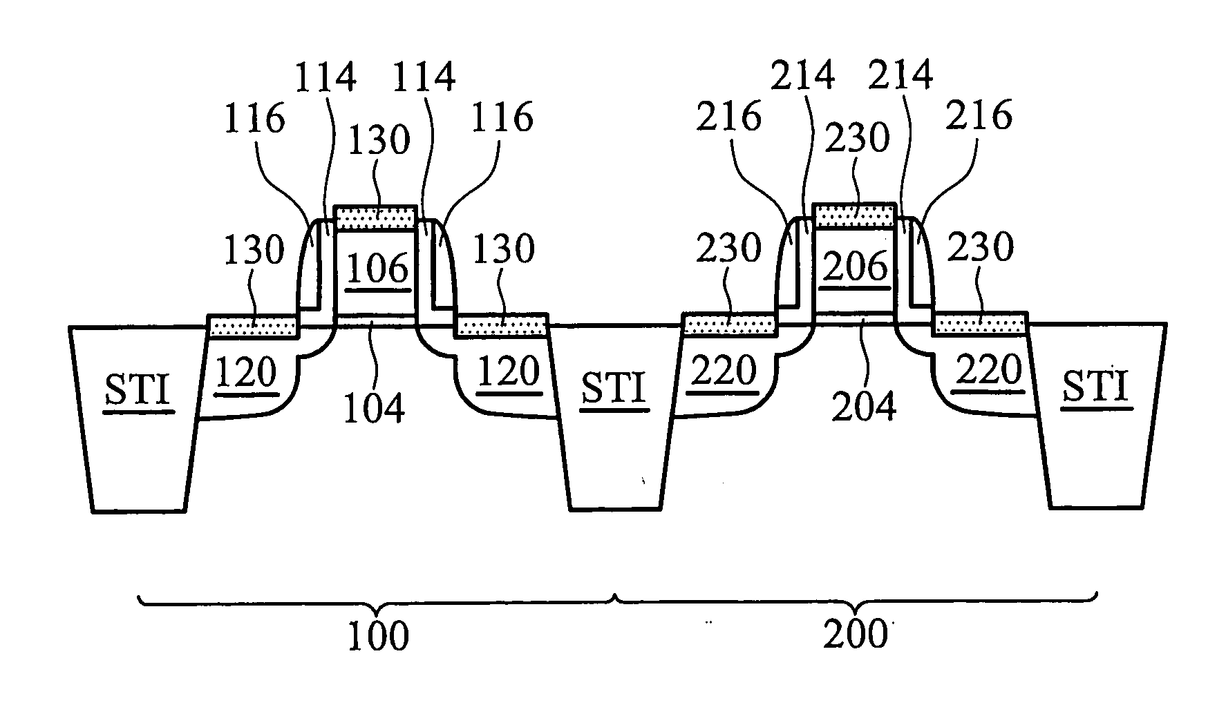
[0023] The making and using of the presently preferred embodiments are discussed in detail below. It should be appreciated, however, that the present invention provides many applicable inventive concepts that can be embodied in a wide variety of specific contexts. The specific embodiments discussed are merely illustrative of specific ways to make and use the invention, and do not limit the scope of the invention.

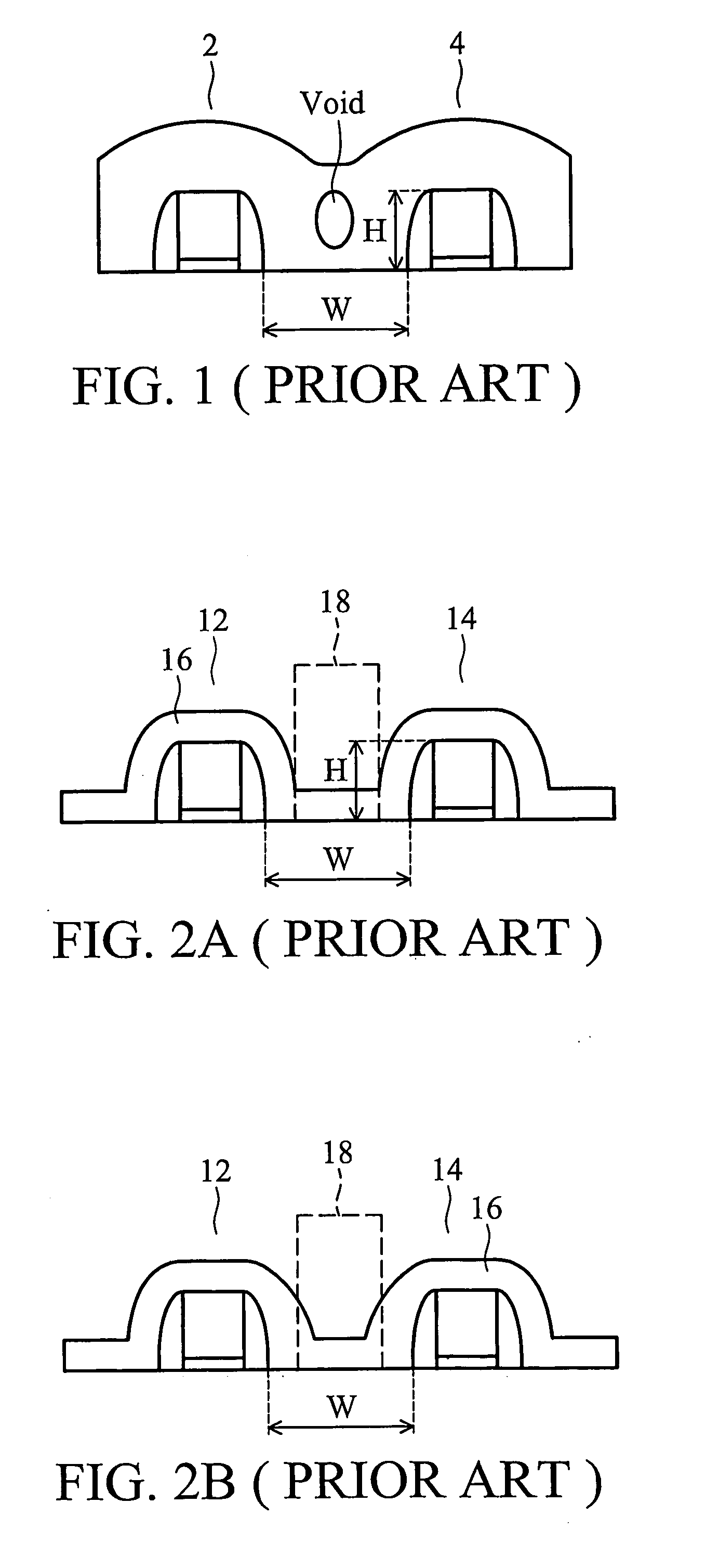
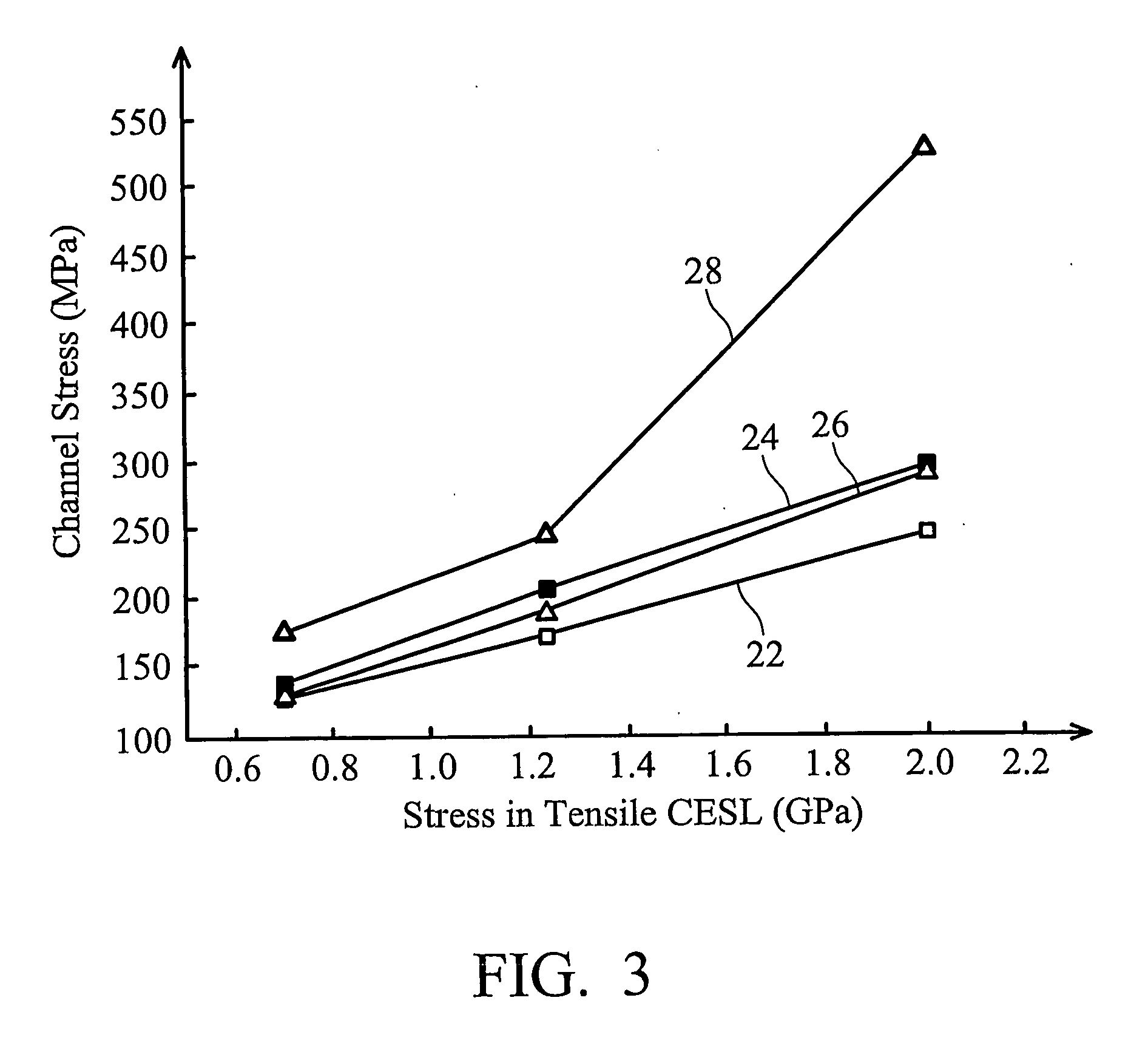
[0024] Simulations have been performed to analyze the correlation between channel stress and gate spacers and contact etch stop layers (CESLs). The results are shown in FIG. 3, wherein channel stresses in the channel length direction are shown as a function of the inherent stresses in CESL layers. Lines 22 and 24 were obtained from MOS devices having spacers with a thickness of about 450 Å, wherein line 22 was obtained from MOS devices with 300 Å CESLs, and line 24 was obtained from MOS devices with 900 Å CESLs. Lines 26 and 28 were obtained from MOS devices with no spacers...


PUM


Abstract

A semiconductor structure includes a substrate, and a first MOS device on the first region of the substrate wherein the first MOS device includes a first spacer liner. The semiconductor structure further includes a second MOS device on the second region wherein the second MOS device includes a second spacer liner. A first stressed film having a first thickness is formed over the first MOS device and directly on the first spacer liner. A second stressed film having a second thickness is formed over the second MOS device and directly on the second spacer liner. The first and the second stressed films may be formed of a same material.

Description

TECHNICAL FIELD [0001] This invention relates generally to semiconductor devices, and more particularly to structures and manufacturing methods of metal-oxide-semiconductor (MOS) devices with improved gap-filling and contact etch process window. BACKGROUND [0002] The scaling of VLSI circuits is a constant effort. Smaller integrated circuits allow more devices to be formed in one semiconductor chip. Additionally, power consumption and performance are also improved. With circuits becoming smaller and faster, improvement in device driving current is becoming more important, which can be increased by improving carrier mobility. Among efforts made to enhance carrier mobility, forming a stressed channel region is a known practice. The performance of a MOS device can be enhanced through a stressed-surface channel. This technique allows performance to be improved at a constant gate length without adding complexity to circuit fabrication or design. [0003] Research has revealed that a bi-axia...

Claims


Application Information

Patent Timeline
IPC IPC(8): H01L29/94H01L29/76H01L31/00
CPCH01L21/823807H01L29/7843H01L21/823864Y10S438/981
Inventor HSU, JU-WANGKO, CHIH-HSINSHIEH, JYU-HORNGPERNG, BAW-CHINGJANG, SYUN-MING
Owner TAIWAN SEMICON MFG CO LTD
Why Eureka
Try Eureka