Plastic microchip for microparticle analysis and method for manufacturing the same

a microchip and microparticle technology, applied in the field of plastic microchip for microparticle analysis and method for manufacturing the same, can solve the problems of increasing the manufacture cost, affecting the quality of microchips, etc., and achieves the effect of facilitating the observation of samples

Inactive Publication Date: 2007-10-11
INCYTO
View PDF4 Cites 38 Cited by
  • Summary
  • Abstract
  • Description
  • Claims
  • Application Information

AI Technical Summary

Benefits of technology

[0038]Accordingly, the present invention has been made in an effort to solve the above-described drawbacks. In one aspect, the present invention provides a plastic microchip and a method for manufacturing the same that can form a microgrid pattern with a narrow width deeply, clearly and uniformly by forming a negative microgrid pattern on a lower substrate, thus facilitating the observation of sample.

Problems solved by technology

However, the above-described plastic microchip has several drawbacks in that it requires a lot of time and cost for manufacturing the same since a plastic material is melted and put into a mold to form a lower substrate, thus increasing the manufacture cost.
Accordingly, the price of an end product is too high to use the microchip as a disposable.
Moreover, it requires high temperature and high pressure to inject a molten plastic material into a microgrid pattern with a narrow width formed on a mold in order to create a positive microgrid pattern, and further there have been a lot of difficulties in forming a microgrid pattern clearly on the lower substrate.

Method used


Image

  • Plastic microchip for microparticle analysis and method for manufacturing the same
  • Plastic microchip for microparticle analysis and method for manufacturing the same
  • Plastic microchip for microparticle analysis and method for manufacturing the same

Examples


Embodiment Construction

[0069]Hereinafter, reference will now be made in detail to the preferred embodiment of the present invention, examples of which are illustrated in the accompanying drawings, wherein like reference numerals refer to like elements throughout.

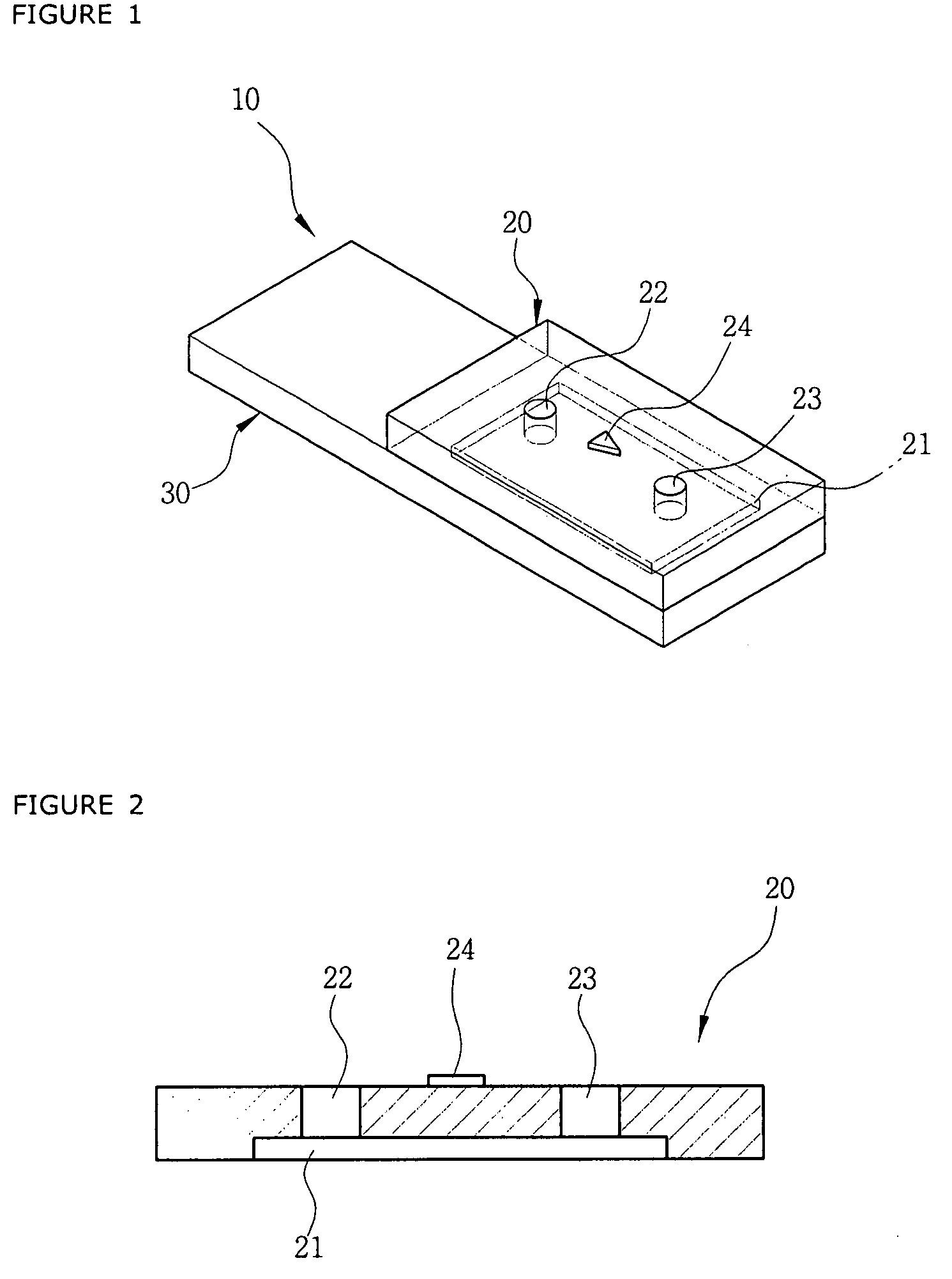
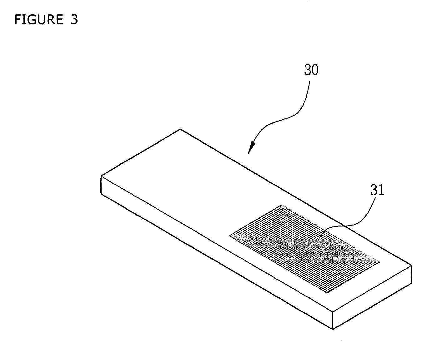
[0070]The present invention relates to a plastic microchip used in counting the number of microparticles contained in a sample of liquid phase such as a solution, an organic solvent, etc. using analysis equipment including an optical microscope, a CCD camera, etc., and a method for manufacturing the same and, more particularly, to a plastic microchip having a negative microgrid pattern for counting the number of microparticles and a method for manufacturing the plastic microchip to which a solvent welding process is applied so as to fix an upper substrate to a lower substrate.

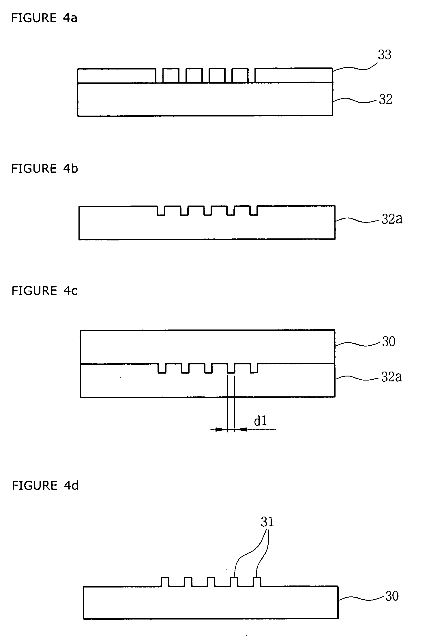
[0071]FIG. 6 is an exploded perspective view of a plastic microchip in accordance with the present invention, and FIGS. 7A and 7B are sectional views of an upper substrate of...


PUM

PropertyMeasurementUnit
heightaaaaaaaaaa
heightaaaaaaaaaa
depthaaaaaaaaaa

Abstract

Disclosed herein is a plastic microchip used in counting the number of microparticles and a method for manufacturing the same and, more particularly, to a plastic microchip including a negative microgrid pattern formed on a lower substrate, a solvent channel and solvent inlets for a solvent welding process, and a method for manufacturing the plastic microchip by injection molding the lower substrate on which a negative microgrid pattern is formed and by injecting a solvent through the solvent inlets so as to fix an upper substrate to the lower substrate.
According to the present invention, it is possible to form a microgrid pattern of a relatively narrow width deeply and uniformly as a negative microgrid pattern is formed on the lower substrate and thereby to provide a clear microgrid pattern, thus facilitating accurate observation of microparticles. Moreover, it is also possible to provide a uniform height of an injection chamber by welding an upper substrate and a lower substrate to each other by a solvent welding process, thus ensuring a more accurate analysis result.

Description

CROSS-REFERENCE TO RELATED APPLICATION[0001]This application claims the benefit under 35 U.S.C. §119(a) on Korean Patent Application No. 10-2006-0032494 filed on Apr. 10, 2007 the entire contents of which are hereby incorporated by reference.BACKGROUND OF THE INVENTION[0002]1. Field of the Invention[0003]The present invention relates to a plastic microchip used in counting or observing microparticles included in a sample of liquid phase and a method for manufacturing the same More particularly, the present invention relates to a plastic microchip including a negative microgrid pattern adapted for counting the number of microparticles and a method for manufacturing the plastic microchip in which a solvent welding process is employed in fixing an upper substrate to a lower substrate.[0004]2. Description of Related Art[0005]In general, microparticles are particles between 1 to 100 μm in size included in a solution and an organic solvent.[0006]Such microparticles may be exemplified by b...

Claims


Application Information

Patent Timeline
Patent Type & Authority Applications(United States)
IPC IPC(8): C12M1/34H01L21/00
CPCB01L3/502707B01L2200/12B81B2201/058B81C1/00119G01N2015/1486B81C2201/036G01N15/1459G01N15/1463G01N15/1484B81C2201/019
Inventor KIM, HYUN JIN
Owner INCYTO
Why Eureka
Try Eureka