Semiconductor apparatus and test method therefor

a semiconductor and apparatus technology, applied in the field of semiconductor apparatus, can solve the problems of increasing circuit size, difficulty in testing a memory chip with different row/column configuration using one bist circuit, and deterioration of quality

Inactive Publication Date: 2007-10-18
RENESAS ELECTRONICS CORP
View PDF10 Cites 24 Cited by
  • Summary
  • Abstract
  • Description
  • Claims
  • Application Information

AI Technical Summary

Benefits of technology

[0021]The present invention uses the high-speed test control circuit capable of selecting a signal transfer rate according to a test speed when accessing and testing the memory circuit through the external terminal. It is thereby possible to test the memory circuit by selecting a signal transfer rate according to a test speed, such as using a signal transfer rate according to high

Problems solved by technology

It is thus difficult to test a memory chip with different row/column configuration using one BIST circuit.
This causes deterioration of quality and increase in circuit size.
This is because an optimal number of rows and columns of a memory, even with the same number of bits, can vary by manufacturing process (corresponding design rule), and it is thus difficult for one BIST to conform to a memory chip with a different number of rows and columns in the test that is conducted based on the number of rows and co

Method used


Image

  • Semiconductor apparatus and test method therefor
  • Semiconductor apparatus and test method therefor
  • Semiconductor apparatus and test method therefor

Examples


first embodiment

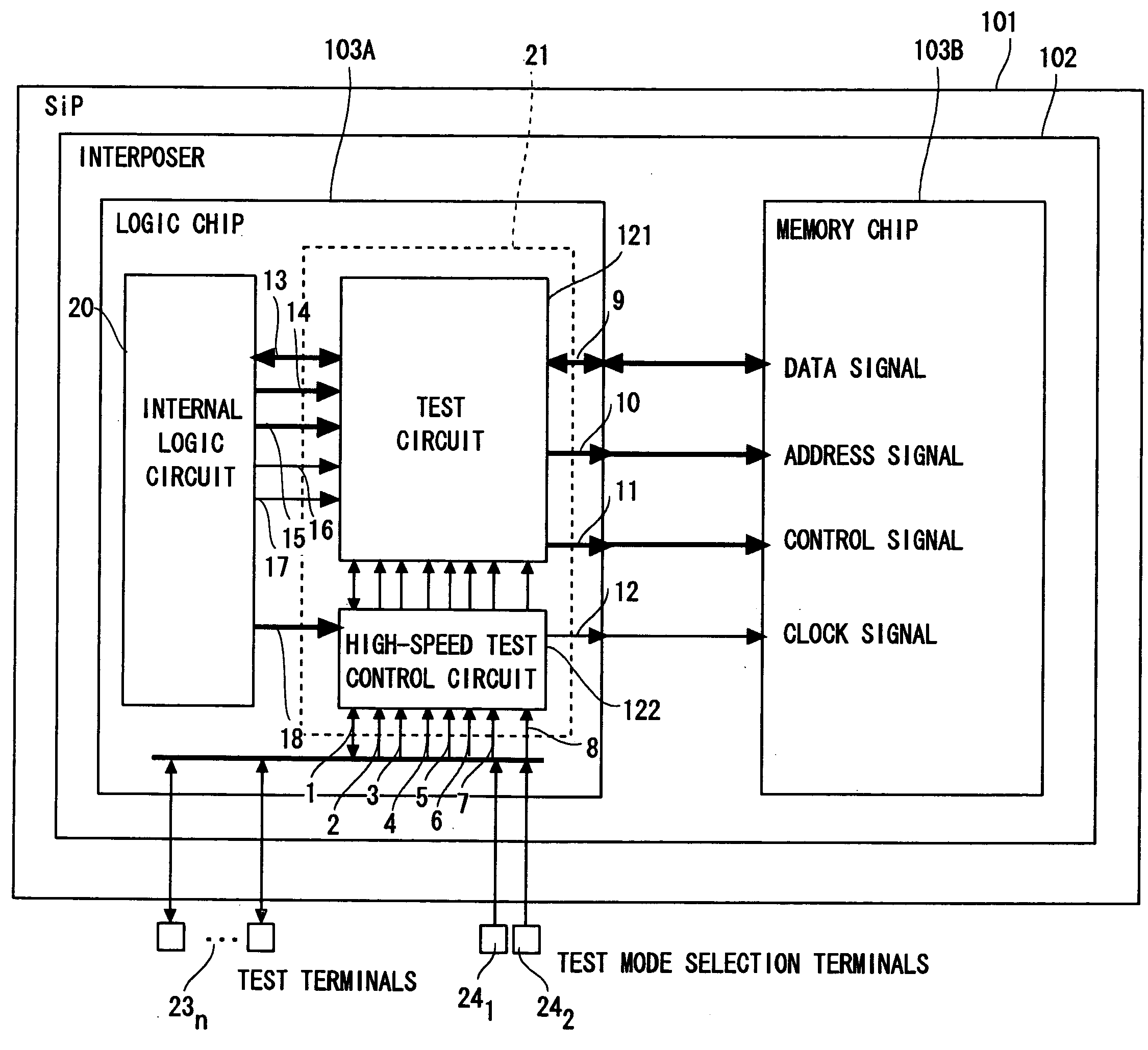
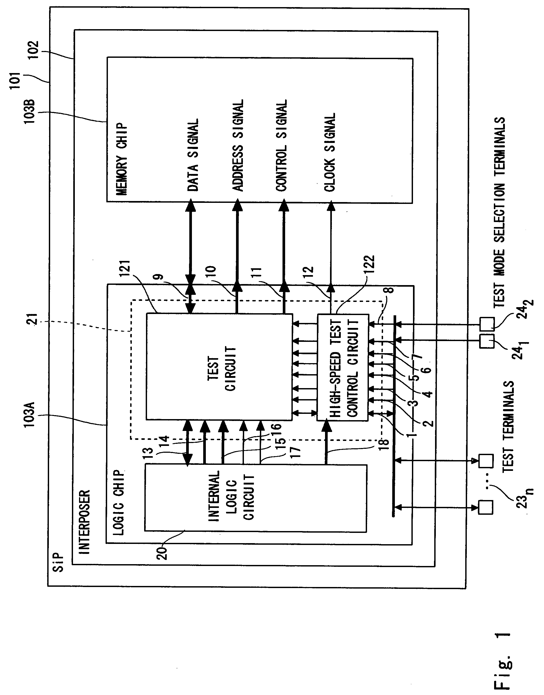
[0040]FIG. 1 is a block diagram showing a semiconductor apparatus according to a first embodiment of the present invention. A SiP semiconductor apparatus (which is referred to hereinafter as “SiP”) 101 of this embodiment includes a logic chip 103A and a memory chip 103B placed on an organic substrate (interposer) 102.

[0041]The logic chip 103A includes an internal logic circuit 20 and a test processor 21 and is connected with a plurality of test terminals 23n and two test mode selection terminals 241 and 242 as external terminals. The test terminals 23n and the test mode selection terminals 241 and 242 may be set as either dedicated external terminals or shared external terminals in view of the number of external terminals used by a user. The logic chip 103A and the memory chip 103B are connected directly by a bump, a wire or the like, and each terminal of the memory chip 103B is not drawn as an external terminal.

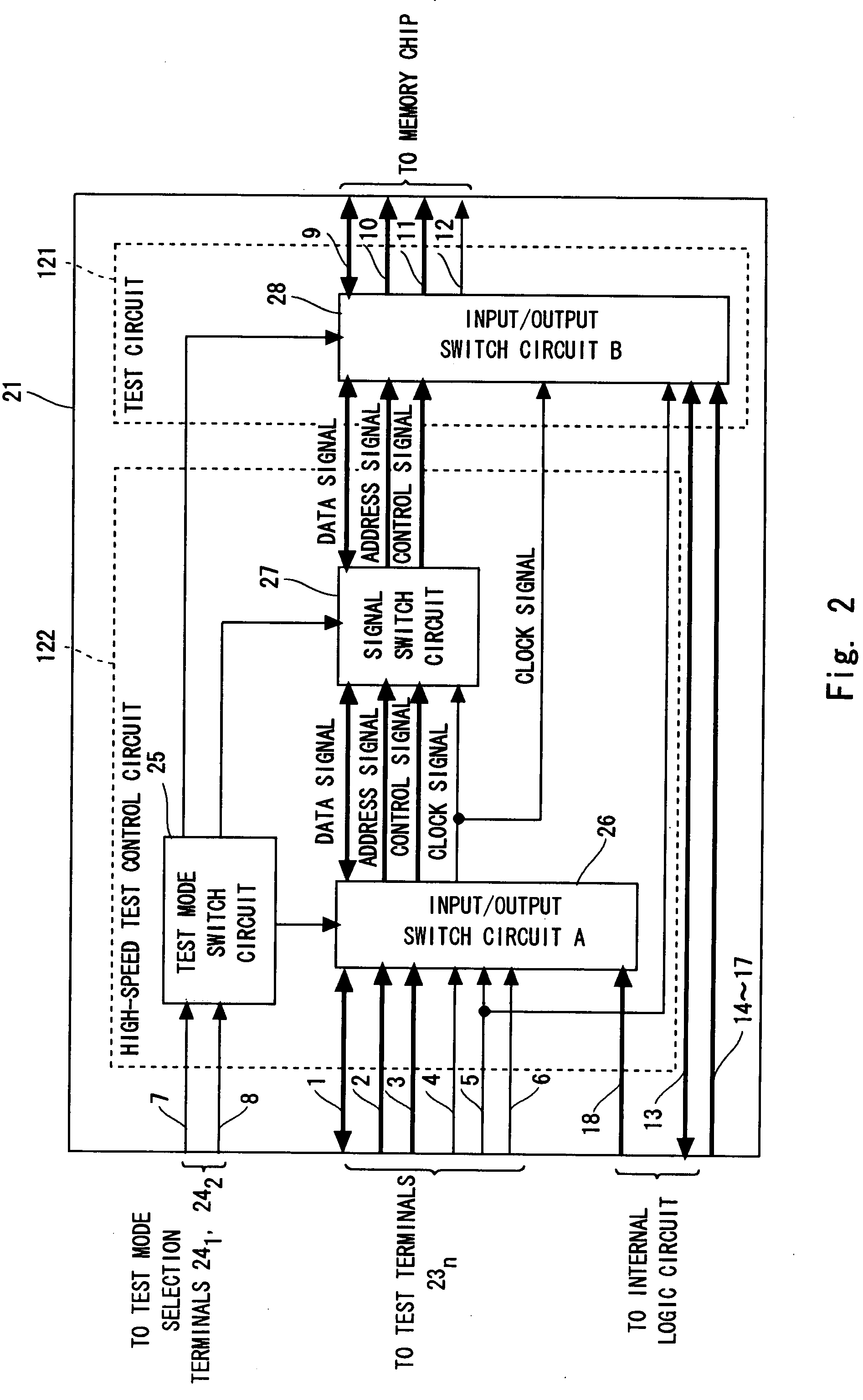
[0042]The test processor 21 of this embodiment includes a test circuit ...

second embodiment

[0081]FIG. 7 is a view showing a semiconductor apparatus according to a second embodiment of the present invention. The second embodiment is different from the first embodiment shown in FIG. 1 in that two memory chips are connected with a single logic chip on the same data bus. With the two memory chips connected, it is still possible to perform high-speed testing of the memory chips 103B and 103C independently of each other simply by forming the circuit configuration that can perform READ operation independently on the memory chips 103B and 103C.

third embodiment

[0082]FIG. 8 is a view showing a semiconductor apparatus according to a third embodiment of the present invention. The third embodiment is different from the second embodiment shown in FIG. 7 in that two test processors 21A and 21B are placed for the two memory chips 103B and 103C so that a test circuit is connected one to one therewith. Although the memory chips 103B and 103C are tested independently of each other in the second embodiment, this embodiment enables the simultaneous high-speed testing of the memory chips 103B and 103C to thereby reduce a test time.

[0083]The present invention can thus provide a semiconductor apparatus and a test method of the semiconductor apparatus capable of high-speed testing at a desired operation frequency. Accessing the memory circuit means controlling read / write operation and observing read data on the memory circuit.

[0084]Thus, as described in the foregoing, the present invention has the following advantages:

1. It is capable of testing the memo...


PUM


Abstract

A SiP includes a logic chip and a memory chip. The memory chip includes a memory circuit to be tested, and the logic chip includes an internal logic circuit and a test processor electrically connected therewith. The test processor is connected with an access terminal of the memory circuit and supplies a test signal input from an external terminal to the access terminal to thereby test the memory circuit. The test processor includes a high-speed test control circuit to adjust signal delay and supplies a test signal from the external terminal to the access terminal through the high-speed test control circuit when performing high-speed test at an actual operation speed.

Description

BACKGROUND OF THE INVENTION[0001]1. Field of the Invention[0002]The present invention relates to a SiP (System in a Package) semiconductor apparatus that incorporates a logic chip and a memory chip into a common package and a test method for the same.[0003]2. Description of Related Art[0004]BIST (Built-In Self-Test) is a test method for a semiconductor apparatus that conducts self-test using a test pattern generator, a test pattern compressor, a comparator or the like placed inside a device. In the BIST, a test pattern generator generates a test pattern to be supplied to a test target circuit, a test pattern compressor compresses an output pattern from the test target circuit, and a comparator compares the compressed test pattern with an expected output pattern, thereby testing the test target circuit.[0005]Japanese Unexamined Patent Application Publication No. 2003-77296 (Ishikawa) discloses a SiP semiconductor apparatus that incorporates a logic chip and a memory chip into a commo...

Claims


Application Information

Patent Timeline
IPC IPC(8): G01R31/28G06F11/00
CPCG11C29/028G11C29/16G11C2029/0401G11C29/50012G11C29/36G11C29/14G11C2029/3602
Inventor HATTORI, TAKASHIHASHIDUME, YUMIKONISHINO, TATSUHIROIKEDA, KOUJI
Owner RENESAS ELECTRONICS CORP
Why Eureka
Try Eureka