Opto-thermal annealing methods for forming metal gate and fully silicided gate field effect transistors

a field effect transistor and metal gate technology, applied in the field of metal can solve the problems of thermal exposure limitations of fully silicided gate field effect transistors, excessive gate leakage, and inability to meet the requirements of the device,

Active Publication Date: 2007-10-25
TAIWAN SEMICON MFG CO LTD
View PDF7 Cites 408 Cited by
  • Summary
  • Abstract
  • Description
  • Claims
  • Application Information

AI Technical Summary

Benefits of technology

[0011] One method for forming a metal gate field effect transistor in accordance with the invention includes forming a metal gate upon a gate dielectric formed over a semiconductor substrate, and using at least the metal gate as a mask to form a source / drain region into the semiconductor substrate. In accordance with this method, the metal gate is selected to have an opto-thermal annealing radiation reflectivity to avoid opto-thermal annealing damage to the metal gate and metal gate to gate dielectric interface when opto-thermal annealing the source / drain region. This particular method also includes opto-thermal annealing the source / drain region to form an annealed source / drain region while avoiding opto-thermal annealing damage to the metal gate and metal gate to gate dielectric interface.

Problems solved by technology

However, continued scaling of field effect transistor devices presents difficulties insofar as further reduction of the physical gate dielectric thickness leads to excessive gate leakage.
As a result of the increased effective gate dielectric thickness, field effect transistor device performance is compromised.
However, a major impediment for implementation of metal gate field effect transistors is thermal stability of a metal gate electrode and an interface between the metal gate and the gate dielectric.
Fully silicided gate field effect transistors may, under certain circumstances, also have thermal exposure limitations.

Method used


Image

  • Opto-thermal annealing methods for forming metal gate and fully silicided gate field effect transistors
  • Opto-thermal annealing methods for forming metal gate and fully silicided gate field effect transistors
  • Opto-thermal annealing methods for forming metal gate and fully silicided gate field effect transistors

Examples


Embodiment Construction

[0019] The invention, which provides laser annealing methods for forming metal gate field effect transistors and fully silicided gate field effect transistors, is described in further detail below. The drawings, which are provided for illustrative purposes and are not necessarily drawn to scale, are described in further detail above.

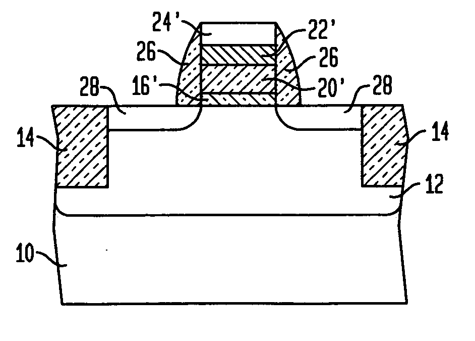
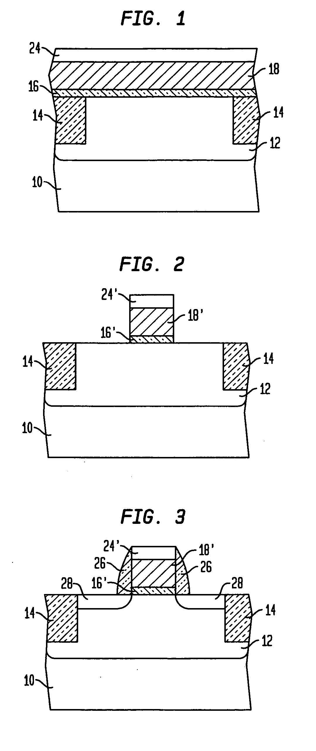
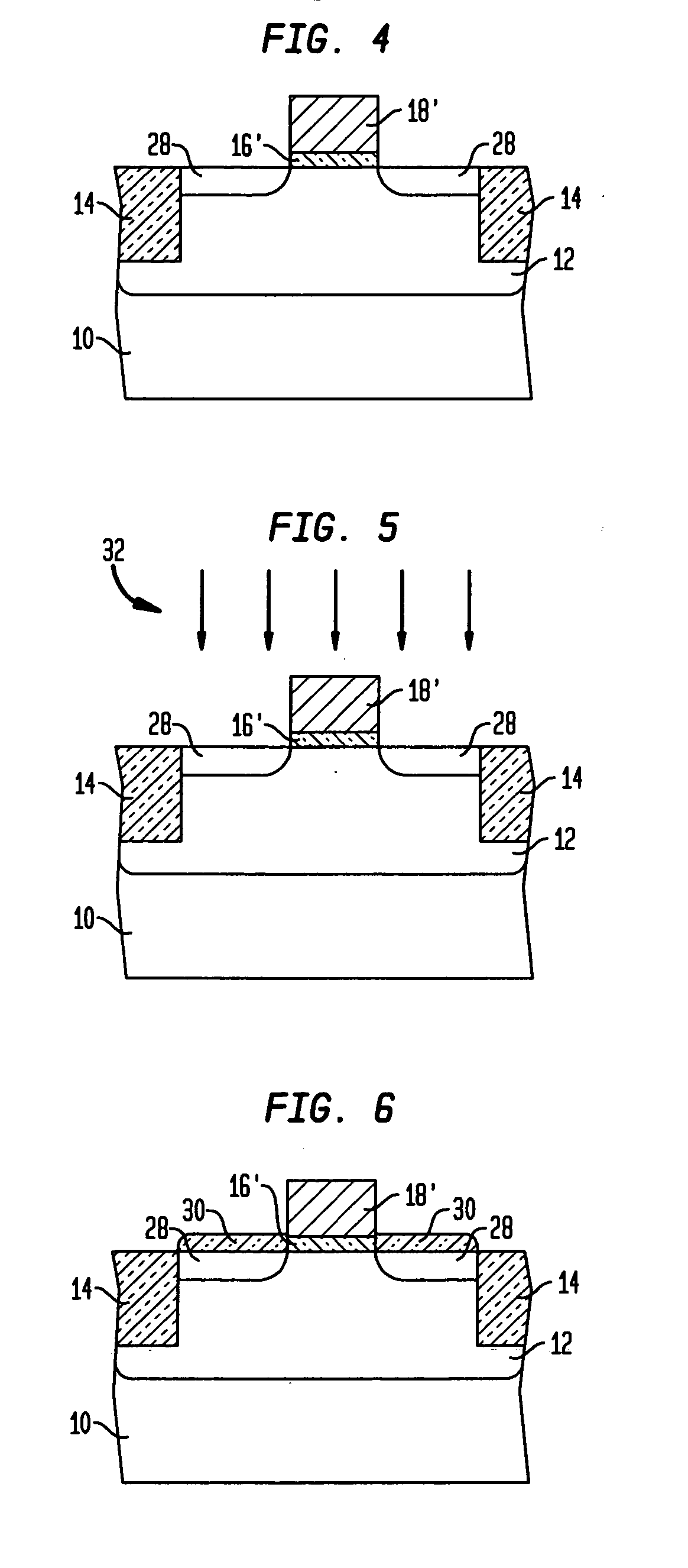
[0020]FIG. 1 to FIG. 6 show a series of schematic cross-sectional diagrams illustrating the results of progressive stages in fabricating a metal gate field effect transistor in accordance with an embodiment of the invention. FIG. 1 shows a schematic cross-sectional diagram of the metal gate field effect transistor at an early stage in its fabrication in accordance with the embodiment of the invention.

[0021]FIG. 1 shows a semiconductor substrate 10. A pair of isolation regions 14 is separated by an active region of the semiconductor substrate 10. The active region includes a doped well 12. A gate dielectric material layer 16 is located upon the isolatio...


PUM

PropertyMeasurementUnit
reflectivityaaaaaaaaaa
time periodaaaaaaaaaa
temperatureaaaaaaaaaa

Abstract

An opto-thermal annealing method for forming a field effect transistor uses a reflective metal gate so that electrical properties of the metal gate and also interface between the metal gate and a gate dielectric are not compromised when opto-thermal annealing a source / drain region adjacent the metal gate. Another opto-thermal annealing method may be used for simultaneously opto-thermally annealing: (1) a silicon layer and a silicide forming metal layer to form a fully silicided gate; and (2) a source / drain region to form an annealed source / drain region. An additional opto-thermal annealing method may use a thermal insulator layer in conjunction with a thermal absorber layer to selectively opto-thermally anneal a silicon layer and a silicide forming metal layer to form a fully silicide gate.

Description

BACKGROUND [0001] 1. Field of the Invention [0002] The invention relates generally to semiconductor device fabrication and in particular to the fabrication of field effect transistor (FET) devices. More particularly, the invention relates to opto-thermal annealing methods for fabricating field effect transistor devices. [0003] 2. Description of the Related Art [0004] A field effect transistor comprises a gate electrode that conventionally comprises a polysilicon or polycide material. The gate electrode is located upon a gate dielectric. The gate dielectric is located upon a semiconductor substrate. A pair of source / drain regions is located within the semiconductor substrate and separated by a channel region located beneath and aligned with the gate electrode. The basic field effect transistor device structure, as described above, has been successfully scaled to increasingly smaller dimensions for over forty years. [0005] Field effect transistor device performance may be improved by ...

Claims


Application Information

Patent Timeline
Patent Type & Authority Applications(United States)
IPC IPC(8): H01L21/336H01L21/44
CPCH01L21/268H01L21/2686H01L21/28079H01L21/28088H01L29/665H01L21/28176H01L21/324H01L29/517H01L21/28097
Inventor ALLEN, SCOTT D.CABRAL, CYRIL JR.DEZFULIAN, KEVIN K.FANG, SUNFEIGREENE, BRIAN J.JAMMY, RAJARAOLAVOIE, CHRISTIANLUO, ZHIJIONGNG, HUNGSUNG, CHUN-YUNGWANN, CLEMENT H.ZHU, HUILONG
Owner TAIWAN SEMICON MFG CO LTD
Why Eureka
Try Eureka