

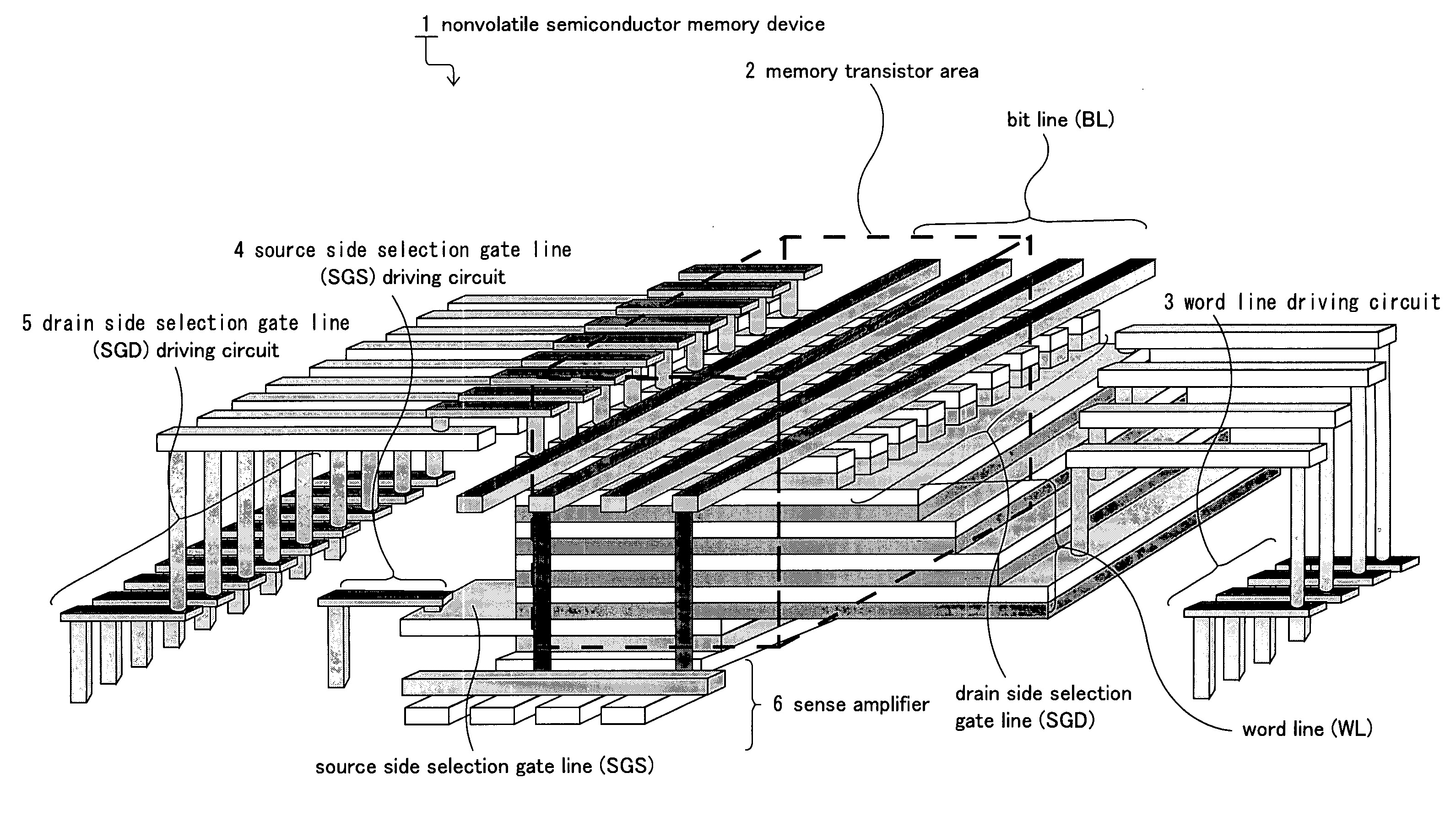
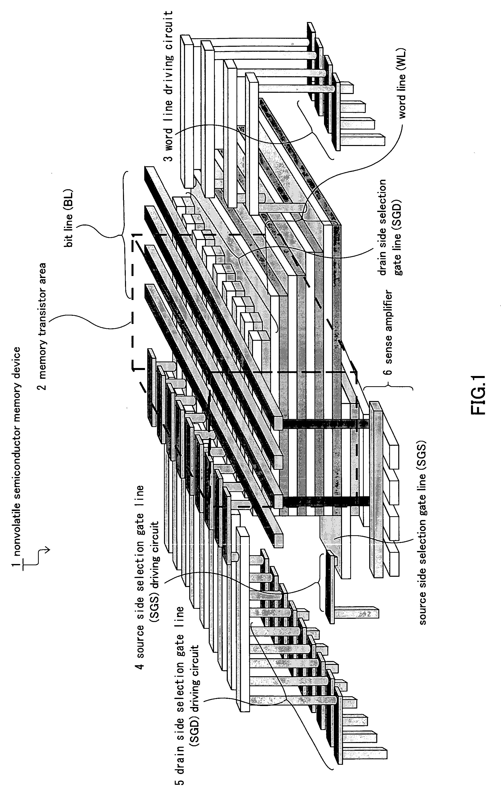
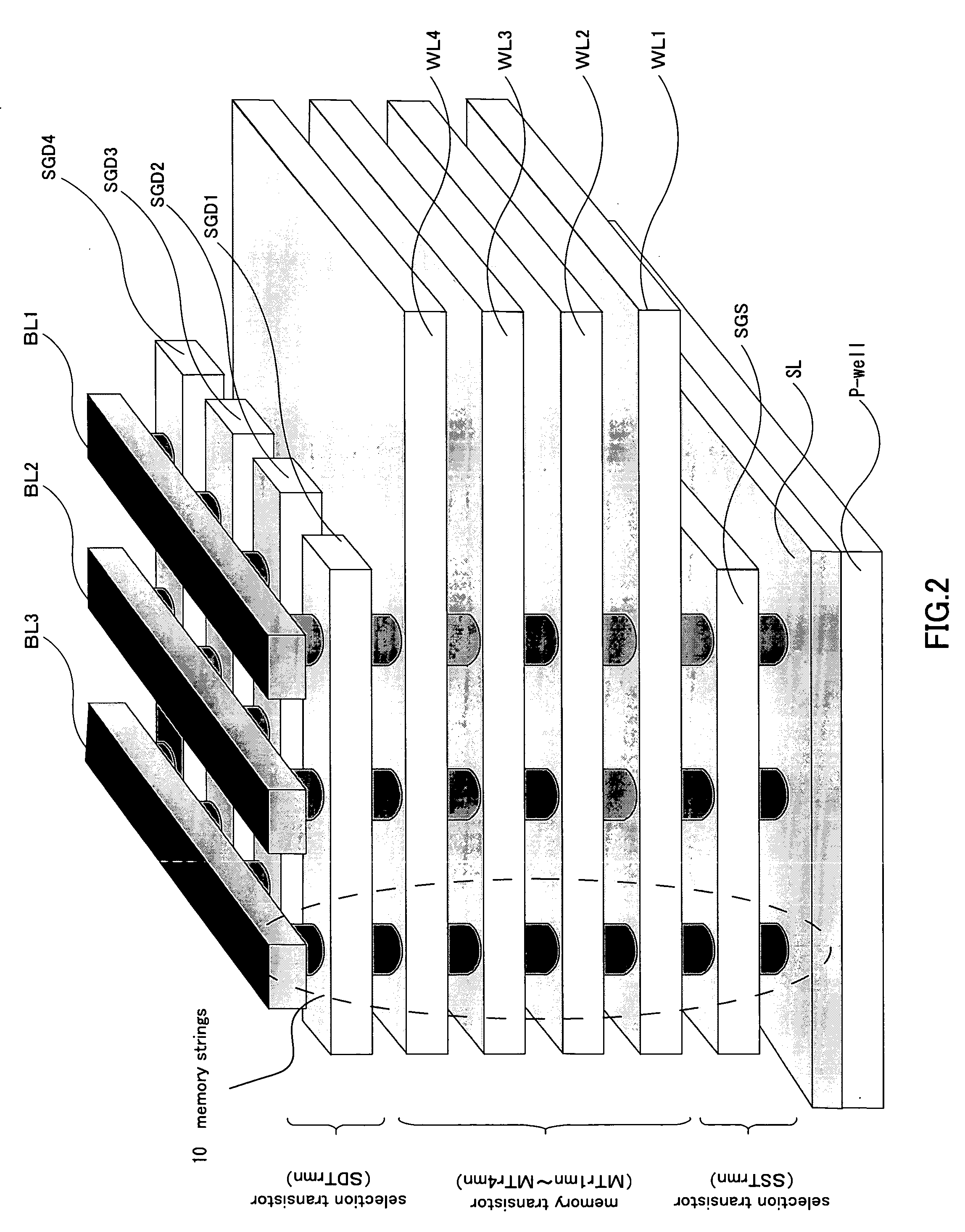
Nonvolatile semiconductor memory device and manufacturing method thereof
a semiconductor memory and non-volatile technology, applied in semiconductor devices, instruments, electrical devices, etc., can solve the problems of reducing the design rules, affecting the quality of semiconductor memory devices,
- Summary
- Abstract
- Description
- Claims
- Application Information
AI Technical Summary
Benefits of technology
Problems solved by technology
Method used
Image

Examples
second embodiment
[0215]In this embodiment, the manufacturing process of another example of the nonvolatile semiconductor memory device of the present invention will be explained using FIG. 45 to FIG. 77. Further in FIG. 45 to FIG. 77, as well as with the first embodiment, a peripheral circuit area, in which peripheral circuits such as a word line driver circuit and a sense amplifier circuit are formed, is shown at the left side; a memory transistor area is shown at the right side. In the memory transistor area, area A part, area B part, and parts equivalent to the cross section of X-X′ and Y-Y′ are shown.
[0216]First, FIG. 45 is shown. By the same method with the first embodiment, STI202a, 202b, 202c, 202d, 202e are formed on the semiconductor substrate 200 are formed (FIG. 45).
[0217]Next, sacrificial oxidation is performed on the substrate surface (not shown in the figures), and after the photo resist patterns are formed at the desired position, boron (B) ions are implanted, and thus P-Well area 204...
third embodiment
[0270]In this embodiment, a film including a nanocrystal film in the charge storage layer of the nonvolatile semiconductor memory device of the present invention. For example, the charge storage layer is set to be a lamination structure configured to a silicon oxide film, a nanocrystal film and a silicon oxide film. As the nanocrystal films, a silicon oxide film including the nanocrystal of the silicon may be used. In the nonvolatile semiconductor memory device according to this embodiment, charges are held in the nanocrystal of the silicon that are disintegrated and distributed in this nanocrystal film.
[0271]Further in this embodiment, the nanocrystal film including the nanocrystal of the silicon is used; however, nanocrystal of metals or the other nanocrystal of conductors, such as cobalt (Co), tungsten (W), silver (Ag) gold (Au), platinum (Pt), etc. In addition, the nanocrystal is also called “metal nano dot” and “nanocrystal”.
[0272]Also in this embodiment, silicon oxide film, na...
fourth embodiment
[0273]In this embodiment, another example of the configuration of the memory transistor area in the nonvolatile semiconductor memory device of the present invention will be explained. In addition, the other configuration will not be explained again, for they are same with the above-described first embodiment, the second embodiment and the third embodiment.
[0274]In the nonvolatile semiconductor memory device according to one embodiment of the present invention, conductor layers and the interlayer films are etched in a taper shape so that steps are formed. Hereby an example, in which two adjacent memory transistor areas are formed, is shown in FIG. 79. FIG. 79 is a diagram, in which the conductor layers of the memory transistor area of the nonvolatile semiconductor memory device of the present invention according to this embodiment are seen from the top part. The conductor layers 300 to 306 show one memory transistor area, in which 300 shows a first conductor layer; 302 shows a second...
PUM
 Abstract
Description
Claims
Application Information