Hybrid integrated circuit device, and method for fabricating the same, and electronic device

a hybrid integrated circuit and integrated circuit technology, applied in the direction of high current circuit adaptation, gain control, association of printed circuit non-printed electric components, etc., can solve the problems of deteriorating affecting the reliability of high-frequency power amplifier modules, and relatively fragile module substrates b>1/b> being liable to develop cracks b>6/b>, so as to facilitate the layout design of external terminals, facilitate communication, and enhance mount rigid rigid

Inactive Publication Date: 2007-11-01
RENESAS ELECTRONICS CORP
View PDF13 Cites 4 Cited by
  • Summary
  • Abstract
  • Description
  • Claims
  • Application Information

AI Technical Summary

Benefits of technology

[0033] The high-frequency power amplifier module (hybrid integrated circuit device) arranged as described in the above item (1) attains the following effectiveness.
[0041] (h) The provision of ground terminals at the four corners of the rectangular module substrate facilitates the layout design of external terminals including the signal terminals and power terminals of the high-frequency power amplifier module, and it also facilitates the layout of wiring lines on the setup board which mounts the module.

Problems solved by technology

However, it was found that this high-frequency power amplifier module develops cracks 6 in the module substrate 1 as shown in FIG. 24, resulting in a degraded reliability of the high-frequency power amplifier module.
In consequence, due to the stress caused by the difference of thermal expansion and contraction between the setup board 3 and electrode terminals 2, the relatively fragile module substrate 1 is liable to develop a crack 6.
The development of crack 6 can deteriorate the reliability of high-frequency power amplifier module.
A green sheet having through-holes needs to be thicker to some extent for the sake of damage-free treatment, and the use of extra green sheet material results in an increased cost of the module.

Method used


Image

  • Hybrid integrated circuit device, and method for fabricating the same, and electronic device
  • Hybrid integrated circuit device, and method for fabricating the same, and electronic device
  • Hybrid integrated circuit device, and method for fabricating the same, and electronic device

Examples


embodiment 1

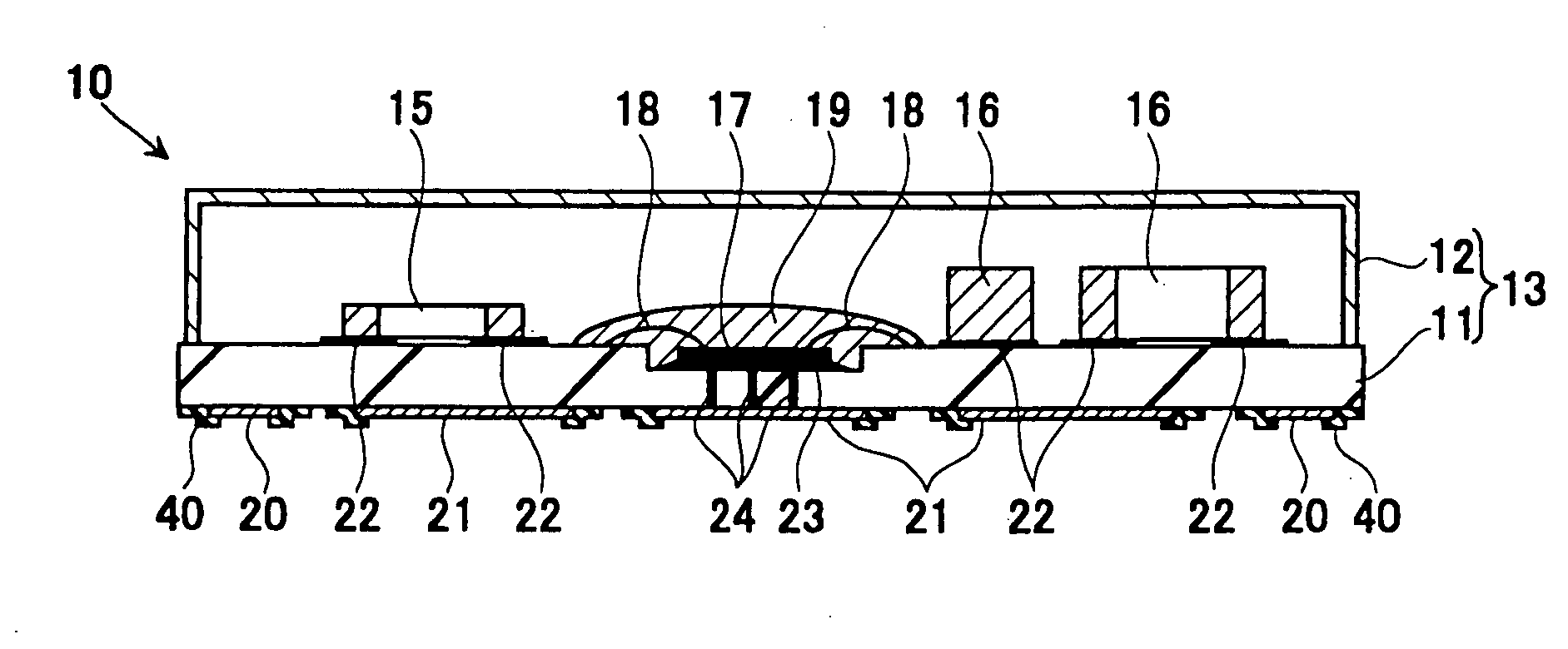
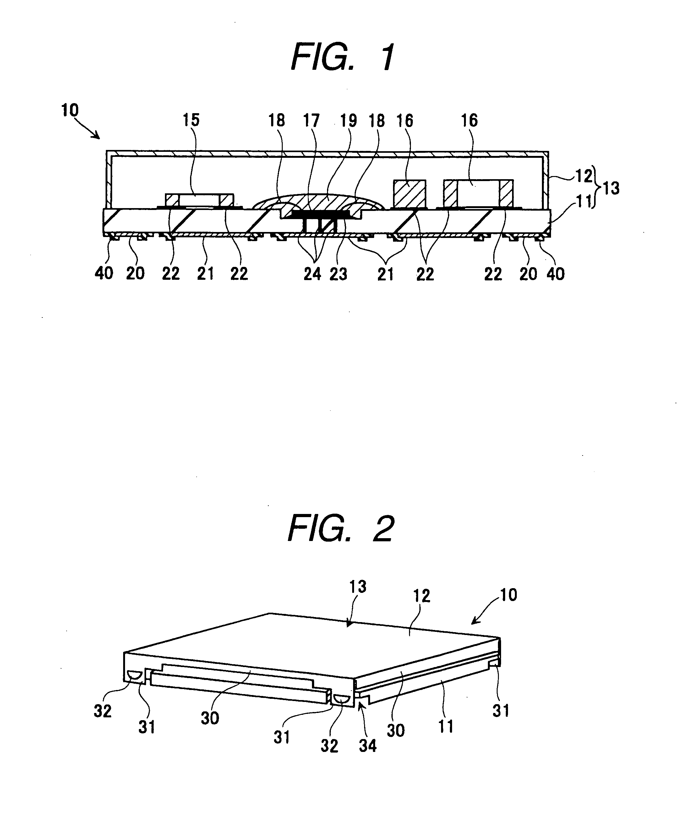
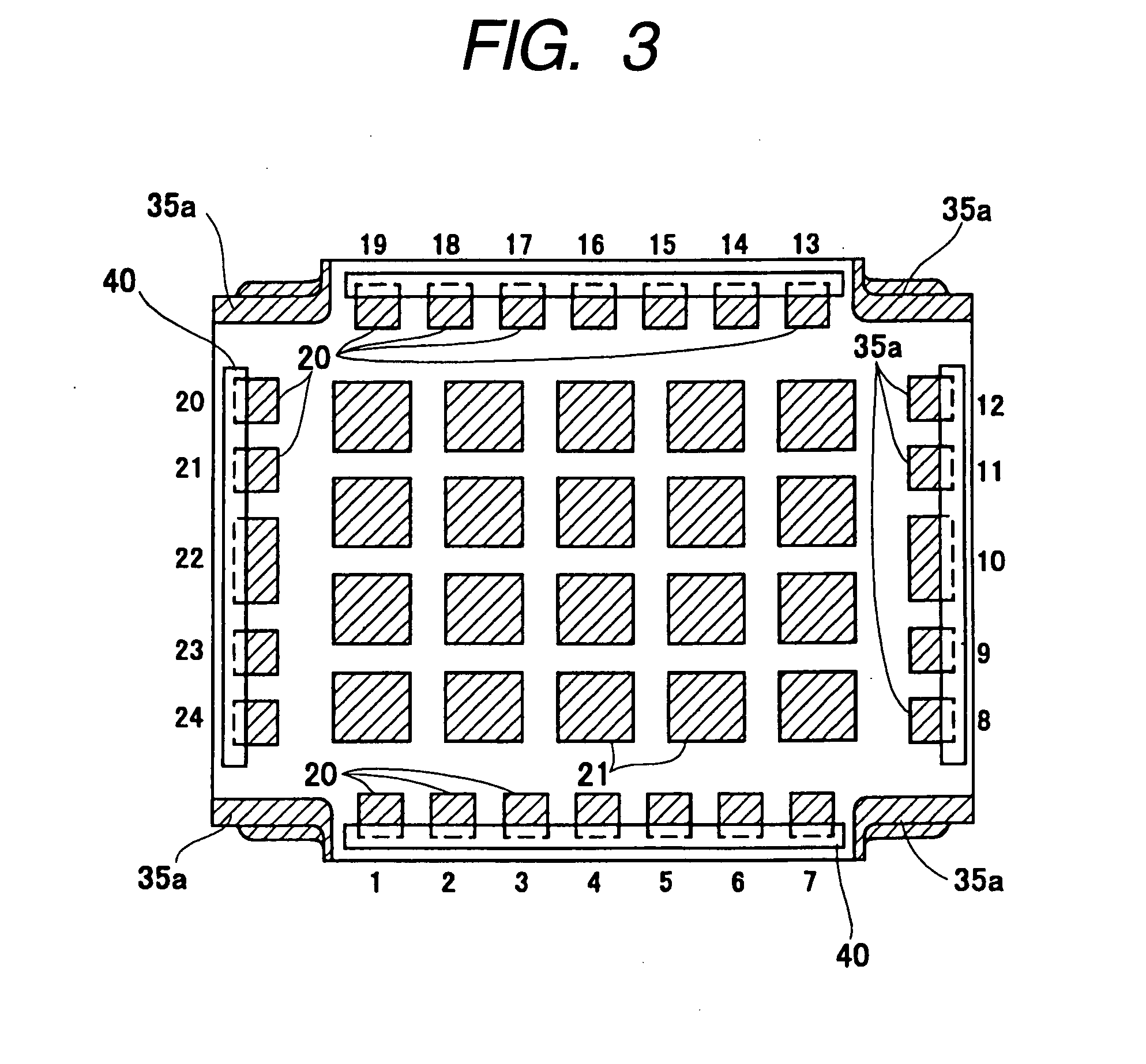
[0067]FIG. 1 through FIG. 17 are diagrams pertaining to a high-frequency power amplifier module and a portable telephone unit which incorporates the module based on an embodiment (embodiment 1) of this invention. Among the figures, FIG. 1 through FIG. 11 are of the high-frequency power amplifier module, and FIG. 12 through FIG. 17 are of the portable telephone unit.

[0068] Explained in this embodiment are a high-frequency power amplifier module, as hybrid integrated circuit device, having amplifying systems for GSM (Global System for Mobile Communication) and DCS (Digital Cellular System), and a wireless communication unit which incorporates the high-frequency power amplifier module.

[0069] The high-frequency power amplifier module 10 has an external appearance of a flat cuboid as shown in FIG. 1 and FIG. 2.

[0070] The high-frequency power amplifier module 10 is structured to have a module substrate 11 which is a ceramic wiring substrate and a cap 12 which is put on one surface (mai...

embodiment 2

[0127]FIG. 18 is a schematic cross-sectional diagram of a high-frequency power amplifier module based on another embodiment (embodiment 2) of this invention. FIG. 19 is a plan view of the bottom of the module substrate of the high-frequency power amplifier module. FIG. 20 is a cross-sectional diagram showing partially the connection of an electrode terminal to the setup board of the high-frequency power amplifier module.

[0128] In this example of the embodiment 2, a protection film 40 is coated around the whole rim of the electrode terminals 20 and power voltage supply terminals 21 as shown in FIG. 18, FIG. 19 and FIG. 20. The embodiment 2 has the same effectiveness as the embodiment 1.

embodiment 3

[0129]FIG. 21 is a plan view of the bottom of a high-frequency power amplifier module based on still another embodiment (embodiment 3) of this invention. In this example of the embodiment 3, hook stoppers 33 are disposed at the middle of the sides of the module substrate 11. In correspondence to these hook stoppers 33, the cap 12 has its hook support arms 31 (not shown) located at the middle of the sides of the cap 12. In the embodiment 3, the foot print on the terminal side can be connected without jutting out of the module substrate, allowing the user's circuit board to have an increased setup area.


PUM


Abstract

A hybrid integrated circuit device having high mount reliability comprises a module substrate which is a ceramic wiring substrate, a plurality of electronic component parts laid out on the main surface of the module substrate, a plurality of electrode terminals laid out on the rear surface of the module substrate, and a cap which is fixed to the module substrate to cover the main surface of the module substrate. The electrode terminals include a plurality of electrode terminals which are aligned along the edges of the module substrate and power voltage supply terminals which are located inner than these electrode terminals. The electrode terminals aligned along the substrate edges are coated, at least in their portions close to the substrate edge, with a protection film having a thickness of several tens micrometers or less. Connection reinforcing terminals consist of a plurality of divided terminals which are independent of each other, and are ground terminals.

Description

[0001] This application is a continuation of U.S. application Ser. No. 11 / 302,144, filed Dec. 14, 2005, which is a continuation of U.S. application Ser. No. 10 / 470,549, filed Jul. 30, 2003, now abandoned, which was a U.S. national stage application of PCT / JP02 / 00534, filed Jan. 25, 2002.TECHNICAL FIELD [0002] The present invention relates to a hybrid integrated circuit device and an electronic device which incorporates the hybrid integrated circuit device, and particularly to a technique which is applied effectively to a high-frequency power amplifier module, which is used for the transmitter of a wireless communication unit such as a cellular telephone unit, and to a wireless communication unit (portable telephone unit) which incorporates the high-frequency power amplifier module. BACKGROUND ART [0003] One known hybrid integrated circuit device is a high-frequency power amplifier module which is used for the wireless communication section of mobile communication units such as autom...

Claims


Application Information

Patent Timeline
Patent Type & Authority Applications(United States)
IPC IPC(8): H01L23/48H01L23/10H01L23/367H01L23/498H01L23/66H01L25/16H03G3/30H05K1/02H05K1/14H05K1/18H05K3/34
CPCH01L23/10H01L23/13H01L2924/1305H01L2924/01019H01L2224/73265H01L2224/32225H01L24/48H01L23/3121H01L23/3677H01L23/49811H01L23/49838H01L23/49894H01L23/50H01L23/66H01L25/165H01L2224/48227H01L2924/01078H01L2924/09701H01L2924/13091H01L2924/15153H01L2924/15165H01L2924/16152H01L2924/19041H01L2924/19105H01L2924/3025H03G3/3042H05K1/0263H05K1/141H05K1/183H05K3/3405H05K3/3436H05K3/3452H05K2201/099H05K2201/09909H05K2201/10371H01L2924/00012H01L2924/00H01L24/73H01L2224/451H01L2924/00014H01L2924/14H01L2924/181H01L2224/45099H01L2224/05599H01L25/04
Inventor MORIYAMA, SHINJIYAMADA, TOMIO
Owner RENESAS ELECTRONICS CORP
Why Eureka
Try Eureka