Plasma display panel (PDP)

Inactive Publication Date: 2007-11-08
SAMSUNG SDI CO LTD
View PDF7 Cites 3 Cited by
  • Summary
  • Abstract
  • Description
  • Claims
  • Application Information

AI Technical Summary

Benefits of technology

[0009]The present invention provides a Plasma Display Panel (PDP) capable of reducing an address discharge voltage between address electrodes and Y electrodes, suppressing address discharge delay, and improving brightness.
[0019]According to another aspect of the present invention, a Plasma Display Panel (PDP) is provided including: a first substrate; a second substrate spaced apart from the first substrate and facing the first substrate; barrier ribs arranged between the first and second substrates and defining discharge cells where a discharge occurs; discharge electrode pairs comprising X electrodes and Y electrodes extending across the discharge cells; floating electrodes arranged closer to the Y electrodes than to the X electrodes; address electrodes extending across the discharge cells and intersecting the discharge electrode pairs within the discharge cells, distances between the Y electrodes and portions of the address electrodes facing the Y electrodes being shorter than distances between the X electrodes and portions of the address electrodes facing the X electrodes; and phosphor layers arranged within the discharge cells.
[0020]Each of the floating electrodes are preferably electrically separated to prevent electrical signals from being received by the floating electrodes.

Problems solved by technology

This results in an increase in driving voltage and a decrease in the luminous efficiency.
Thus, this resolution fails to achieve stable driving.

Method used


Image

  • Plasma display panel (PDP)
  • Plasma display panel (PDP)
  • Plasma display panel (PDP)

Examples


Embodiment Construction

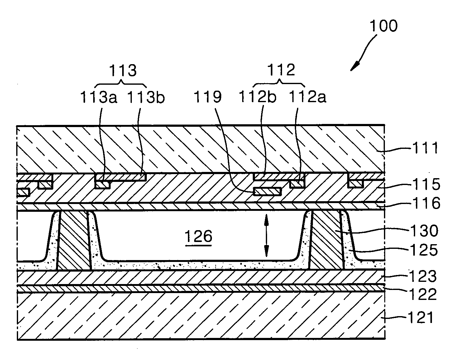
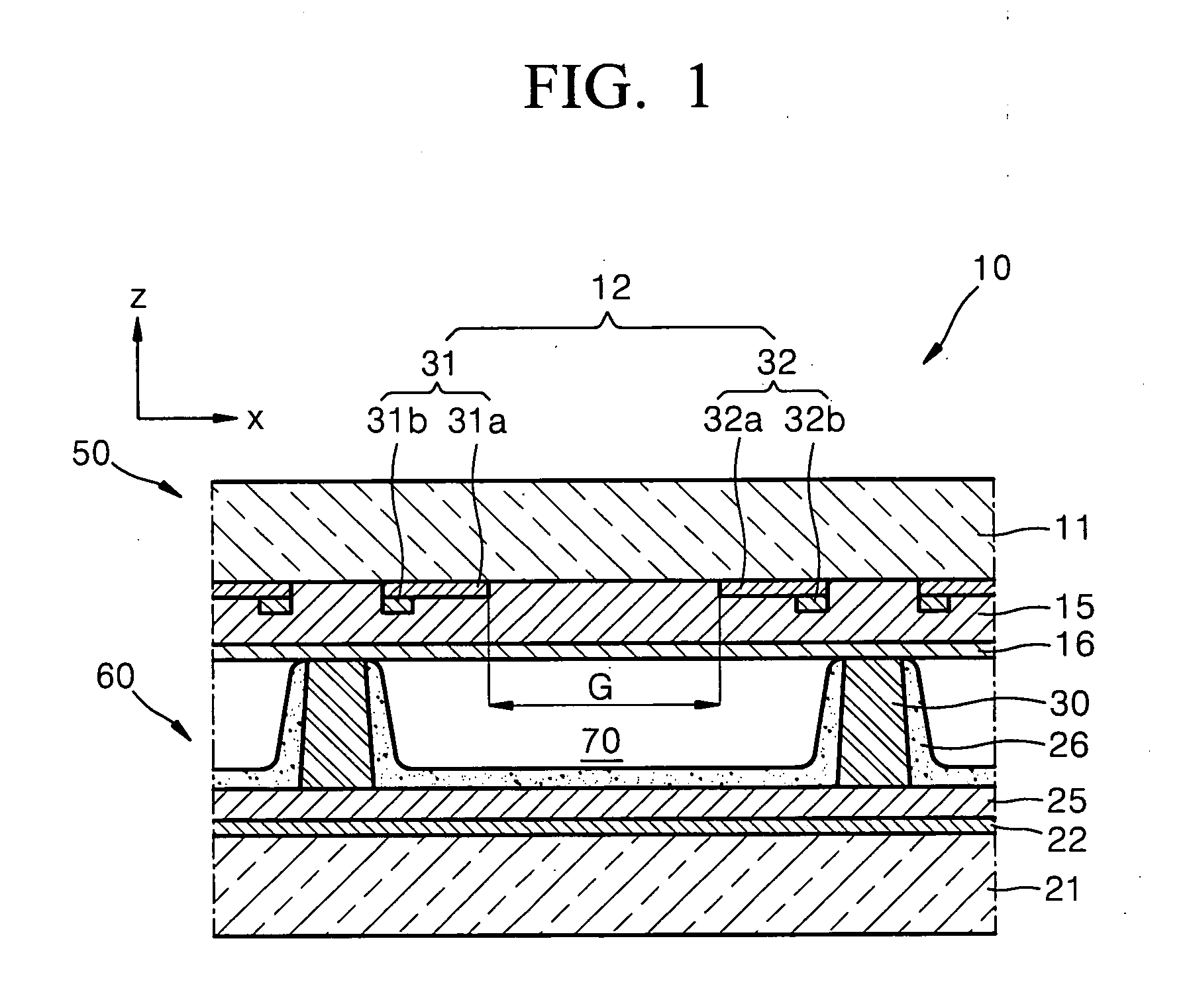
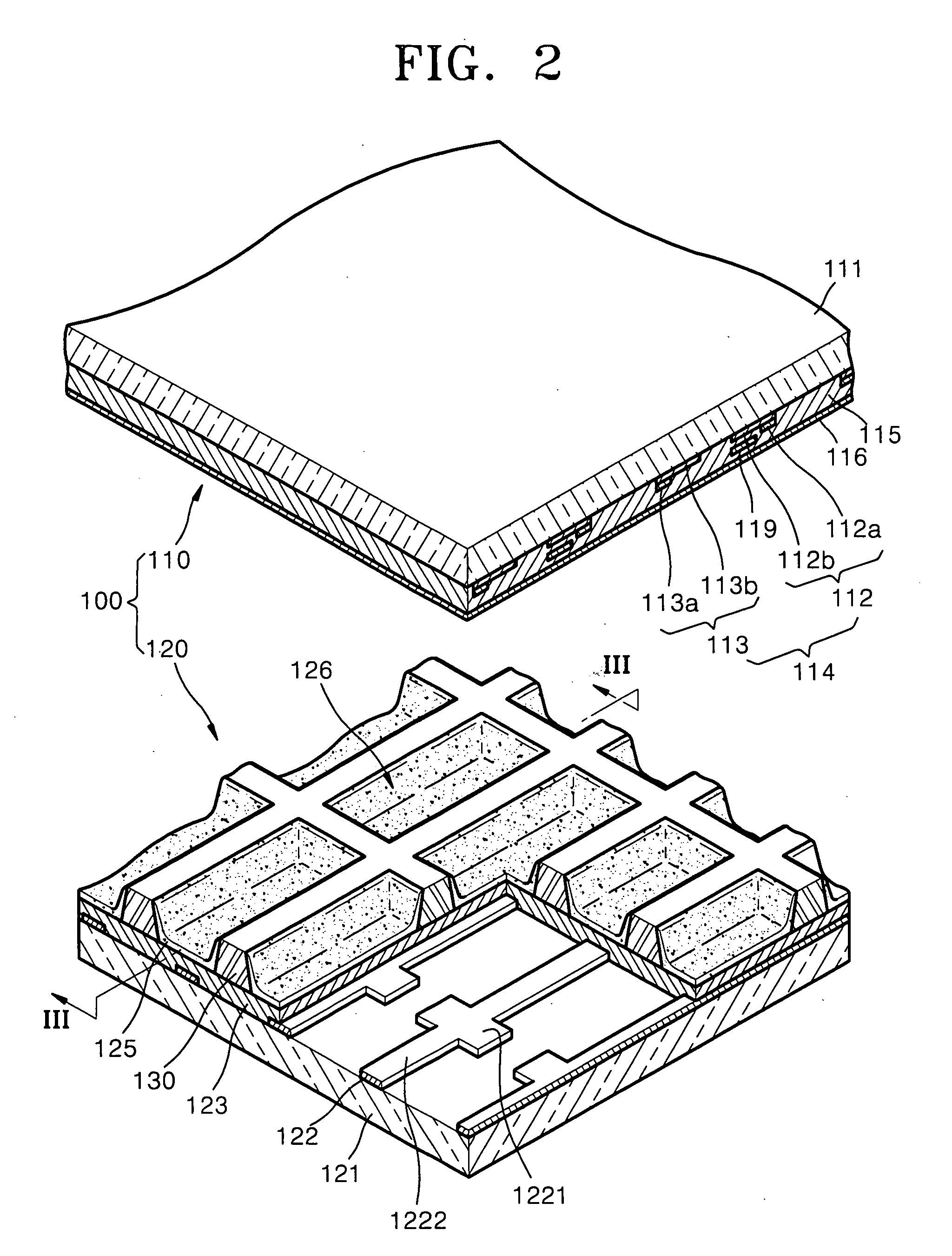
[0031]As illustrated in FIG. 1, a AC PDP 10 includes an upper plate 50 displaying an image to users and a lower plate 60 coupled to the upper plate 50, the lower plate 60 and the upper plate 50 being parallel to each other. Sustain electrode pairs 12, each having an X electrode 31 and a Y electrode 32, are arranged on a front substrate 11 of the upper plate 50. Address electrodes 22 are arranged on a rear substrate 21 of the lower plate60 that faces the front substrate 11 on which the sustain electrode pairs 12 are arranged, and intersect the electrodes 31 and 32 on the front substrate 11. A first dielectric layer 15 and a second dielectric layer 25 are respectively formed on the front substrate 11, including the sustain electrode pairs 12, and the rear substrate 21, including the address electrodes 22, to bury the electrodes 12 and 22. A protection layer 16, which is typically formed of MgO, is arranged on the rear surface of the first dielectric layer 15. Barrier ribs 30, securing...


PUM


Abstract

A Plasma Display Panel (PDP) capable of reducing an address discharge voltage between address electrodes and Y electrodes, suppressing an address discharge delay, and improving brightness includes: a first substrate, a second substrate spaced apart from the first substrate and facing the first substrate, barrier ribs arranged between the first and second substrates and defining discharge cells where a discharge occurs, discharge electrode pairs including X electrodes and Y electrodes extending across the discharge cells, floating electrodes arranged closer to the Y electrodes than to the X electrodes, address electrodes extending across the discharge cells and intersecting the discharge electrode pairs within the discharge cells, and phosphor layers arranged within the discharge cells. Portions of the address electrodes facing the Y electrodes are wider than portions of the address electrodes facing the X electrodes, or distances between the Y electrodes and the portions of the address electrodes facing the Y electrodes are shorter than distances between the X electrodes and the portions of the address electrodes facing the X electrodes.

Description

CLAIM OF PRIORITY[0001]This application makes reference to, incorporates the same herein, and claims all benefits accruing under 35 U.S.C. §119 from an application for PLASMA DISPLAY PANEL earlier filed in the Korean Intellectual Property Office on the 4th of May 2006 and there duly assigned Serial No. 10-2006-0040400.BACKGROUND OF THE INVENTION[0002]1. Field of the Invention[0003]The present invention relates to a Plasma Display Panel (PDP), and more particularly, to a PDP in which a discharge is easily initiated and in which a discharge delay is reduced.[0004]2. Description of the Related Art[0005]Plasma Display Panels (PDPs) are display devices which display images by exciting phosphors with ultraviolet (UV) rays generated during a gas discharge. PDPs have attracted considerable attention as a next-generation thin display device that can be easily manufactured in a large size and display high-resolution images.[0006]Such PDPs are classified into Direct Current (DC), Alternating C...

Claims


Application Information

Patent Timeline
IPC IPC(8): H01J17/49
CPCH01J11/12H01J11/30H01J2211/361H01J2211/265H01J11/32H01J11/26
Inventor JUNG, EUN-YOUNGAHN, JEONG-CHULL
Owner SAMSUNG SDI CO LTD
Why Eureka
Try Eureka