Light emitting device using plasma discharge

a technology of light emitting devices and plasma, which is applied in the direction of gas discharge vessels/containers, gas-filled discharge tubes, holders and dispensers, etc., can solve the problems of increasing discharge voltage, increasing discharge voltage, and easy deterioration of fluorescent layers, so as to reduce discharge voltage and improve luminous efficiency

Inactive Publication Date: 2006-08-03
SAMSUNG ELECTRONICS CO LTD
View PDF9 Cites 8 Cited by
  • Summary
  • Abstract
  • Description
  • Claims
  • Application Information

AI Technical Summary

Benefits of technology

[0014] Embodiments of the present disclosure may provide a plasma-discharge light emitting device capable of reducing discharge voltage and improving luminous efficiency.

Problems solved by technology

Although it has high luminous efficiency, the facing discharge light emitting device has a disadvantage that its fluorescent layer can be easily deteriorated due to plasma.
However, in this case, there is a problem of increase in the discharge voltage.

Method used


Image

  • Light emitting device using plasma discharge
  • Light emitting device using plasma discharge
  • Light emitting device using plasma discharge

Examples


first embodiment

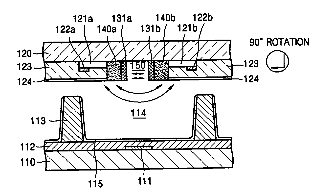
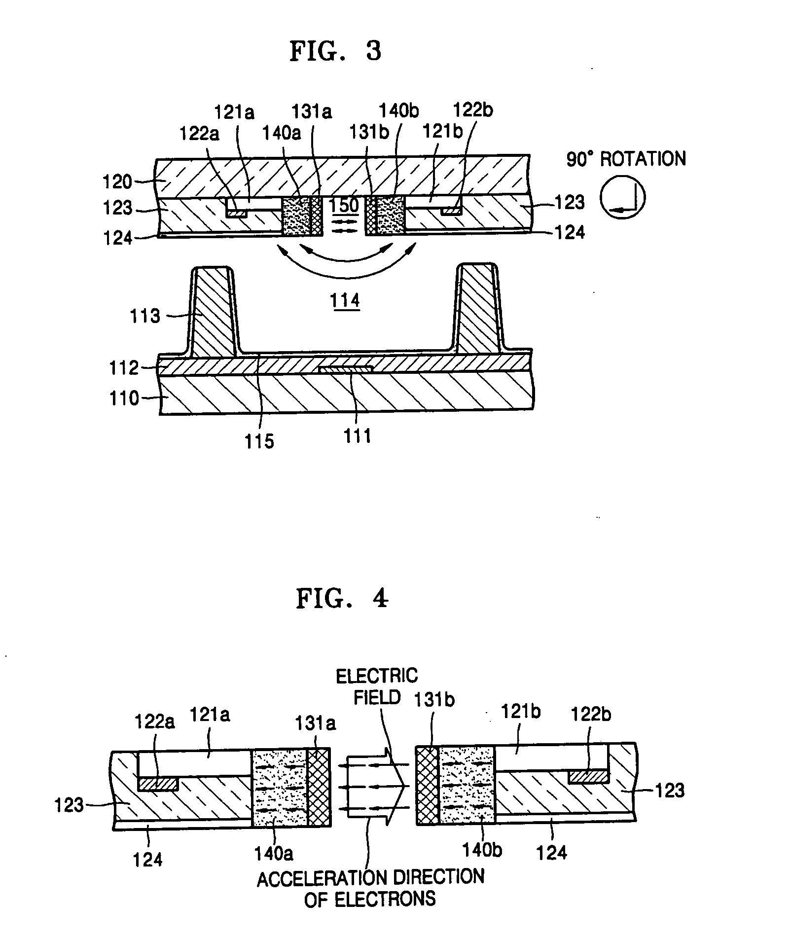
[0039]FIG. 3 is a cross sectional view of a plasma display panel according to the present disclosure. The plasma display panel may include rear and front panels separated from each other in a predetermined interval. A plurality of barrier ribs 113 may be provided between the rear and front panels. The barrier ribs 113 partition a space between rear and front panels to form a plurality of discharge cells 114 where plasma discharge may be generated. In addition, the barrier ribs 113 prevent electrical and optical crosstalk between adjacent discharge cells 114. The discharge cells 114 may be filled with a discharge gas emitting ultraviolet (UV) light at the plasma discharge. The discharge gas may be generally a mixture of Ne and Xe. Red (R), green (G) and blue (B) fluorescent layers 115 having a predetermined thickness may be coated on inner walls of the respective discharge cells 114. The UV light generated by the discharge may excite the fluorescent layers 115. In turn, the fluoresce...

second embodiment

[0052]FIG. 6 is a cross sectional view of a plasma display panel according to the present invention. The plasma display panel may include rear and front panels separated from each other in a predetermined interval. A plurality of barrier ribs 213 defining discharge cells 114 may be provided between the rear and front panels. The discharge cells 214 may be filled with a discharge gas emitting UV light. Fluorescent layers 215 having a predetermined thickness may be coated on inner walls of the respective discharge cells 214.

[0053] The rear panel may include a rear substrate 210, a plurality of address electrodes 211 formed on an upper surface of the rear substrate 210, and a first dielectric layer 212 formed on the upper surface of the rear substrate 210 to bury the address electrodes 211.

[0054] The front panel may include a front substrate 220 separated from the rear substrate 210 in a predetermined interval, a plurality of pairs of first and second sustain electrodes 221a and 221b ...

third embodiment

[0058]FIG. 7 is a cross sectional view of a plasma display panel according to the present disclosure. The plasma display panel may include rear and front panels separated from each other in a predetermined interval. A plurality of barrier ribs 313 defining discharge cells 314 may be provided between the rear and front panels. The discharge cells 314 may be filled with a discharge gas emitting UV light. Fluorescent layers 315 having a predetermined thickness may be coated on inner walls of the respective discharge cells 314. The rear panel may include a rear substrate 310, a plurality of address electrodes 311 formed on an upper surface of the rear substrate 310, and a first dielectric layer 312 formed on the upper surface of the rear substrate 310 to bury the address electrodes 311. The front panel may include a front substrate 320 separated from the rear substrate 310 in a predetermined interval, a plurality of pairs of first and second sustain electrodes 321a and 321b provided for...


PUM


Abstract

A plasma-discharge light emitting device is provided. The plasma-discharge light emitting device may include: rear and front panels separated from each other in a predetermined interval, wherein at least one discharge cell may be provided between the rear and front panels, and wherein plasma discharge may be generated in the discharge cells; a pair of discharge electrodes provided on at least one of the rear and front panels for each of the discharge cells; a trench provided as a portion of each of the discharge cells between the pair of the discharge electrodes; and electron-emitting material layers provided on both sidewalls of the trench.

Description

CROSS-REFERENCE TO RELATED PATENT APPLICATION [0001] This application claims the benefit of Korean Patent Application No. 10-2005-0009109, filed on Feb. 1, 2005, in the Korean Intellectual Property Office, the disclosure of which is incorporated herein in its entirety by reference BACKGROUND OF THE DISCLOSURE [0002] 1. Field of the Disclosure [0003] Embodiments of the present disclosure may include a light emitting device using plasma discharge, and more particularly, a light emitting device using plasma discharge capable of reducing discharge voltage and improving luminous efficiency. [0004] 2. Description of the Related Art [0005] In a light emitting device using plasma discharge (hereinafter, referred to as a plasma-discharge light emitting device), the plasma discharge is generated by a direct-current (DC) or alternating-current (AC) voltage applied between two electrodes, ultraviolet (UV) light generated during the discharge process excites fluorescent materials, and an image i...

Claims


Application Information

Patent Timeline
Patent Type & Authority Applications(United States)
IPC IPC(8): H01J17/49
CPCH01J11/12H01J11/28H01J11/38H01J11/40H01J61/54E03C1/14A47K5/02
Inventor LEE, YOUNG-DONGHATANAKA, HIDEKAZUSON, SEUNG-HYUNSHIN, JAI-KWANGKIM, YOUNG-MO
Owner SAMSUNG ELECTRONICS CO LTD
Why Eureka
Try Eureka