Coupled-fed antenna device

a technology of coupled feed and antenna device, which is applied in the structure of elongated active element feed, resonant antenna, radiating element, etc., can solve the problems of occupying circuit board space, reducing the efficiency of matching circuit, so as to achieve simple design, save space, and reduce the cost

Inactive Publication Date: 2007-11-08
AIPTEK INTERNATIONAL INC
View PDF7 Cites 23 Cited by
  • Summary
  • Abstract
  • Description
  • Claims
  • Application Information

AI Technical Summary

Benefits of technology

[0010] To achieve the aforesaid objects, the present invention provides a coupled-fed antenna device comprising a substrate, a signal source, a ground plane, a radiation conductor and a coupling feedline. The substrate has at least a first surface and a second surface which are defined with a first direction and a second direction perpendicular to each other thereon. The signal source is disposed on the first surface to provide wireless signals. The ground plane is electrically grounded and covers at least a part of the area on the second surface of substrate. The radiation conductor is disposed on the second surface of substrate and extends from the ground plane a predetermined first length generally towards the first direction and then turns generally towards the second direction to extend a predetermined second length to form substantially an inverted F antenna configuration. The coupling feedline connects the signal source and the radiation conductor, and consists of at least a first feedline and a second feedline coupled together without contacting each other. One end of the second feedline is connected to a predetermined attachment point on the radiation conductor. The real part of the input impedance of antenna may be adjusted by shifting the attachment point. The first feedline and the second feedline are coupled together by a coupling element, which is substantially serially connected between the signal source and said attachment point. Thus the imaginary part of the antenna input impedance may be adjusted by changing the input impedance of an open stub of the coupling element. As such, a mechanism for adjusting the “real part of impedance” and “imaginary part of impedance” is disposed directly on the antenna by means of “serial connection” without disposing a matching circuit on the system circuit board to eliminate the effect of “imaginary part impedance”, thereby offering the advantages of simpler design, lower cost and space saving.

Problems solved by technology

Such approach however produces limited effect on the imaginary part of antenna impedance.
The cost of matching circuit is relatively high and takes the space of circuit board, thereby leaving room for further improvement.

Method used


Image

  • Coupled-fed antenna device
  • Coupled-fed antenna device
  • Coupled-fed antenna device

Examples


Embodiment Construction

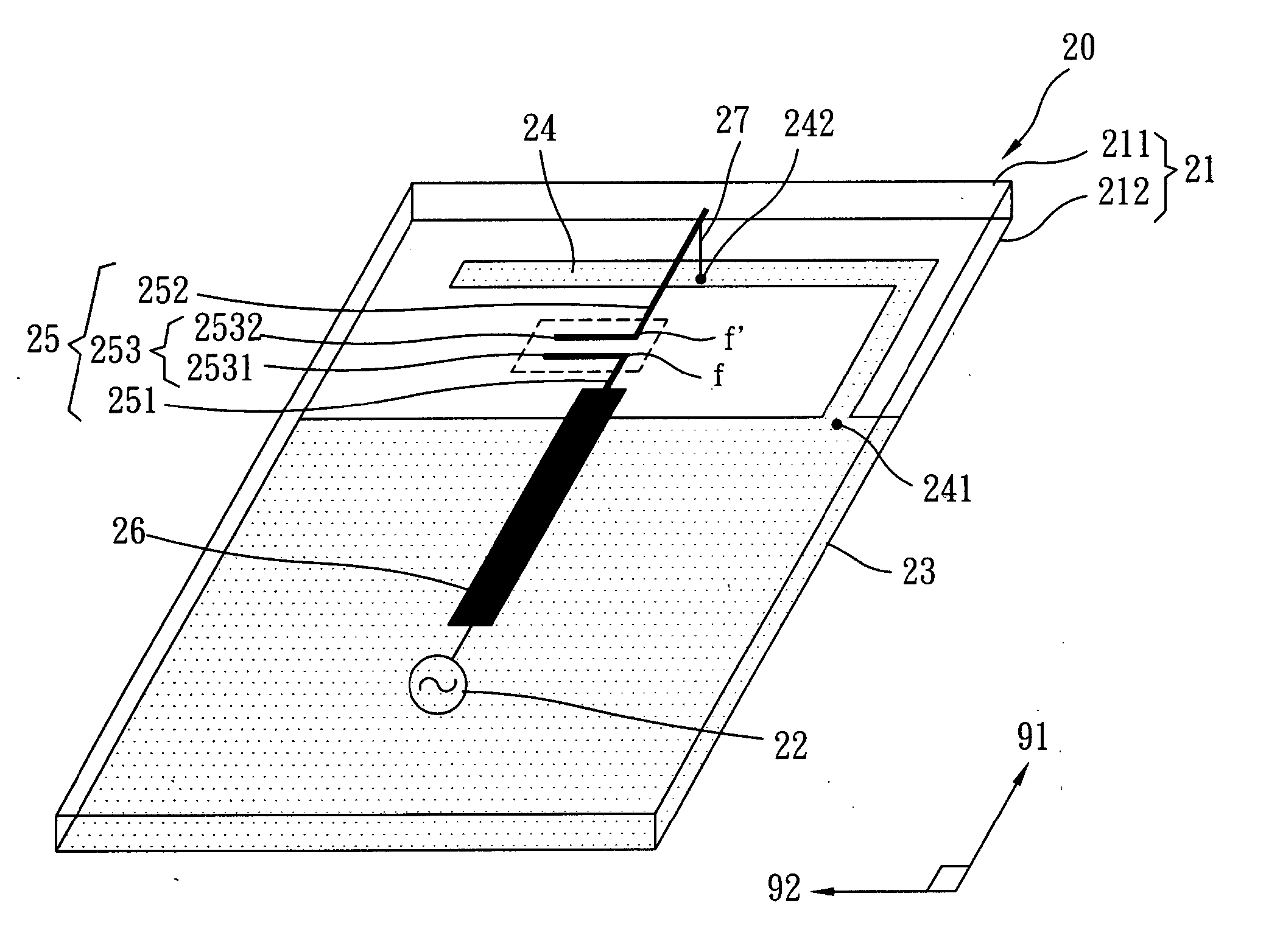
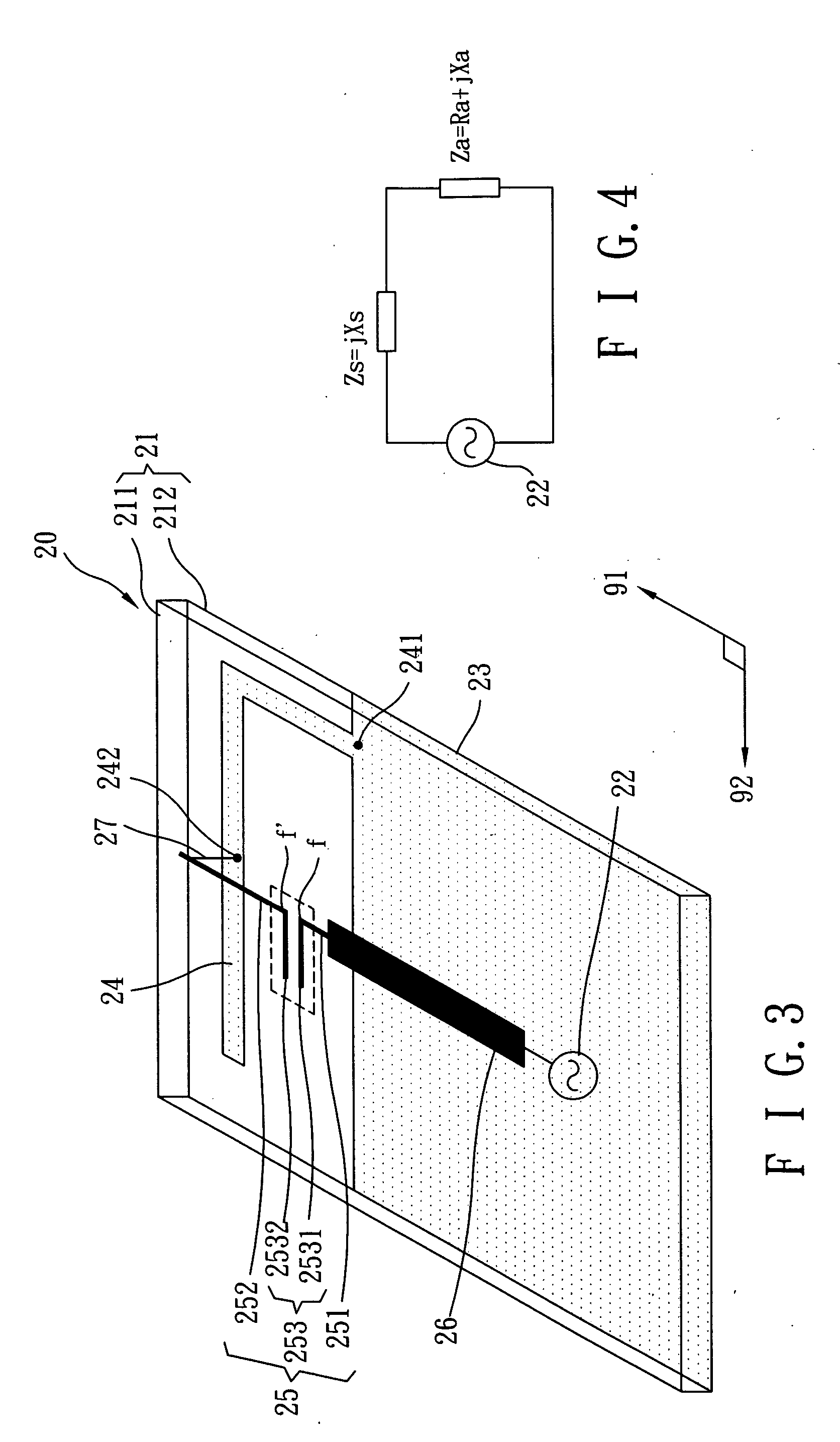
[0020]FIG. 3 shows a perspective view of a coupled-fed antenna 20 according to a first embodiment of the invention. In the first embodiment, the coupled-fed antenna 20 comprises: a substrate 21, a signal source 22, a ground plane 23, a radiation conductor 24, and a coupling feedline 25.

[0021] The substrate 21 is a flat panel made of dielectric material having at least a first surface 211 and a second surface 212. The surfaces 211, 212 of substrate 21 are respectively defined with a first direction 91 and a second direction 92 perpendicular to each other thereon. The first surface 211 and the second surface 212 are substantially the top surface and bottom surface of substrate 21, or an intermediate layer.

[0022] The signal source 22 is disposed on the first surface 211 of substrate 21 to provide high frequency signal for wireless communication. The signal source 22 consists of a plurality of electronic circuits (or integrated circuits) for generating wireless signals. Given that the...


PUM


Abstract

A coupled-fed antenna device comprising a substrate, a signal source, a ground plane, a radiation conductor, and a coupling feedline is disclosed. The substrate has at least a first surface and a second surface, and the signal source is disposed on the first surface. The ground plane is electrically grounded and covers at least partial area on the second surface of substrate. The radiation conductor is disposed on the second surface of substrate and connected to the ground plane. The coupling feedline consists of a first feedline connected to the signal source and a second feedline connected to the radiation conductor. The real part of the antenna input impedance may be adjusted by shifting the attachment point between the second feedline and radiation conductor. The first feedline and the second feedline are coupled together by a coupling element. The imaginary part of the antenna input impedance may be adjusted by changing the input impedance of an open stub of the coupling element.

Description

BACKGROUND OF INVENTION [0001] 1. Field of the Invention [0002] The present invention relates to a kind of coupled-fed antenna device, more particularly a coupled-fed antenna device where its imaginary part of input impedance may be adjusted by disposing a coupling element serially connected to the signal feedline of inverted F antenna. [0003] 2. Description of the Prior Art [0004] The application of wireless communication technology by the military and the private industry is becoming more extensive in recent years. It is also gaining popularity in personal devices. The trends of the future is to equip all electronic devices with the function of wireless communication, for example, computer peripherals, such as wireless mouse, wireless keyboard, and wireless network, or consumer electronics, such as mobile phone, PDA with mobile phone function, bluetooth earpiece, and bluetooth MP3, or even home appliance, such as refrigerator and television. [0005] In products with wireless commun...

Claims


Application Information

Patent Timeline
Patent Type & Authority Applications(United States)
IPC IPC(8): H01Q1/38
CPCH01Q9/42H01Q1/243
Inventor TSENG, WEN JEN
Owner AIPTEK INTERNATIONAL INC
Why Eureka
Try Eureka