Semiconductor integrated circuit device

a technology of integrated circuits and semiconductors, applied in the direction of semiconductor devices, basic electric elements, electrical equipment, etc., can solve the problems of difficult to determine the discharge region, place limitations on the degree of freedom in the layout construction, etc., and achieve the effect of generating the discharge path extremely readily

Inactive Publication Date: 2007-11-15
ELPIDA MEMORY INC
View PDF6 Cites 8 Cited by
  • Summary
  • Abstract
  • Description
  • Claims
  • Application Information

AI Technical Summary

Benefits of technology

[0026]According to the present invention, discharge paths from the wiring layer which is in need of the antenna effect preventive action may be secured without the need of a larger space and without the necessity of significant corrections or alterations in layout. Especially, in case an action against the antenna effect is necessary, part of the reg

Problems solved by technology

Moreover, in case connection has to be made through the uppermost wiring layer, there are placed limitations on the degree of freedom in the layout construction.
However, since the site where it is

Method used


Image

  • Semiconductor integrated circuit device
  • Semiconductor integrated circuit device
  • Semiconductor integrated circuit device

Examples


Embodiment Construction

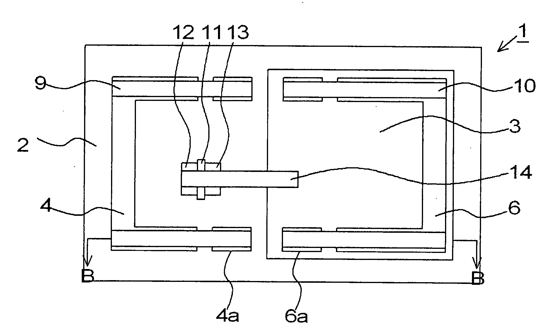
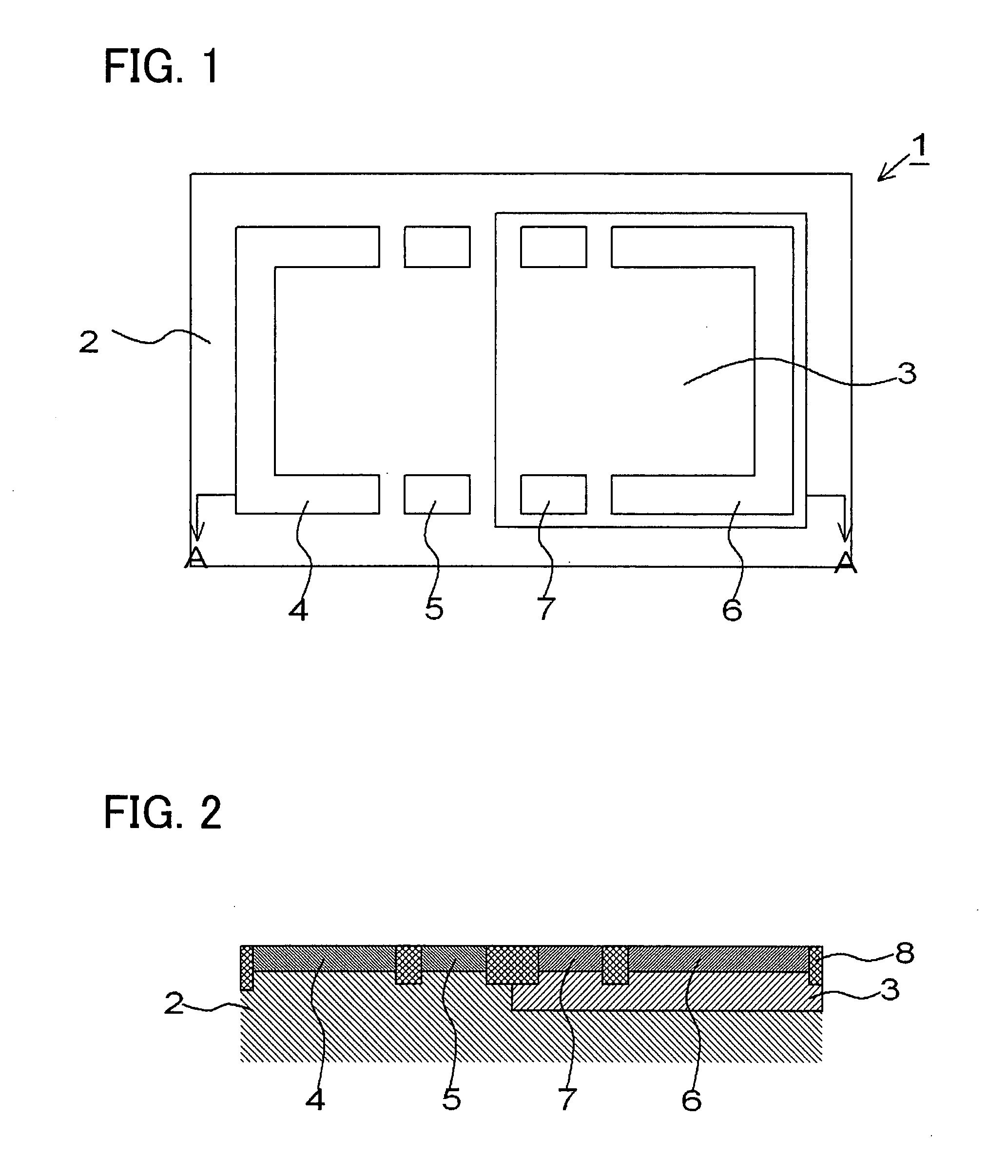
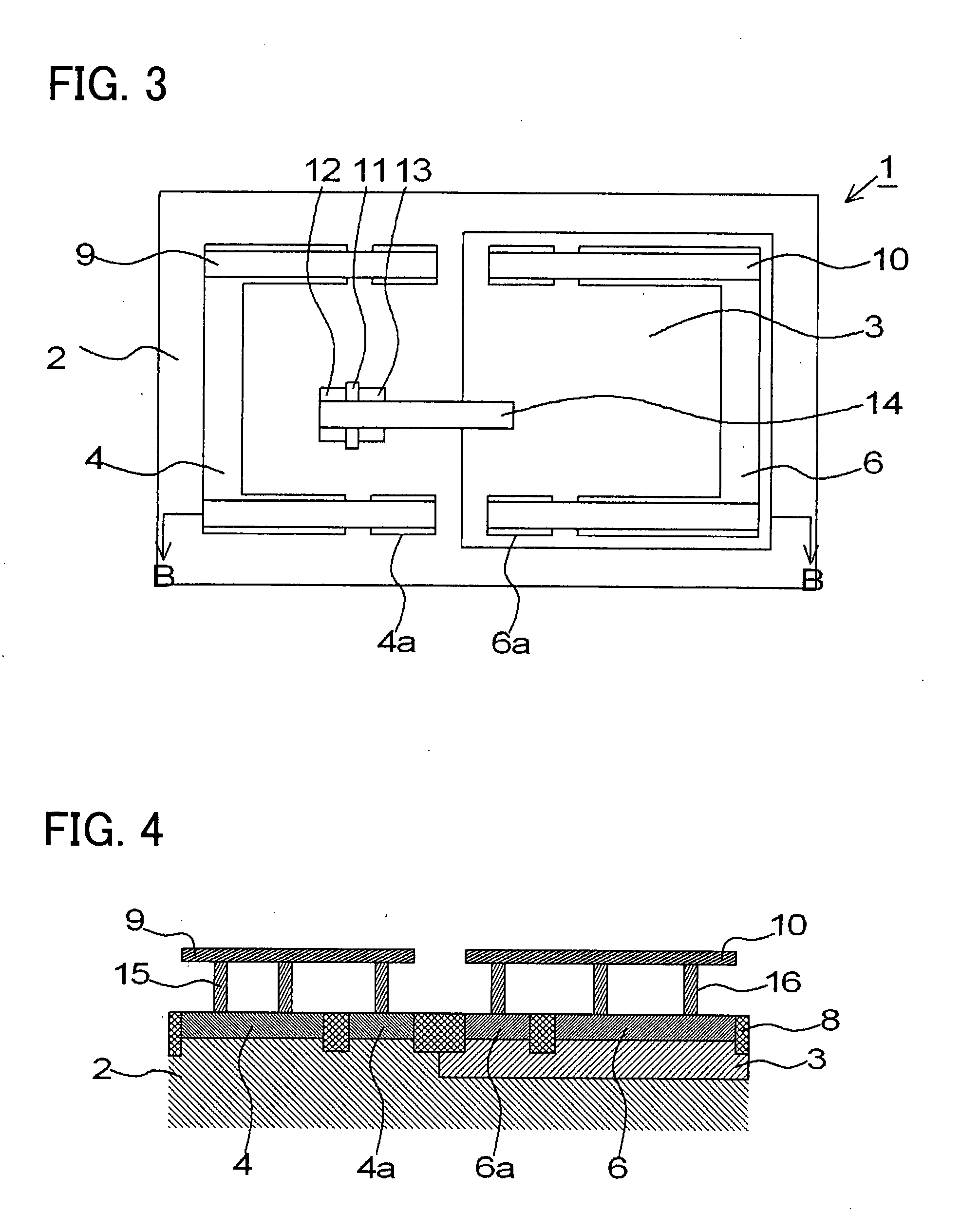
[0041]A semiconductor integrated circuit device and a method for producing the device, according to the present invention, will now be described with reference to a case of a complementary metal oxide semiconductor (CMOS) including a p type semiconductor substrate and an n-well generated in the substrate.

[0042]Referring first to FIGS. 1 and 2, an example of layout of a semiconductor integrated circuit device according to the present invention is now described. FIG. 1 depicts a schematic plan view showing a layout in a semiconductor integrated circuit device 1, and FIG. 2 depicts a schematic cross-sectional view along line A-A of FIG. 1. Meanwhile, in the plan view of the present invention, a silicon oxide film is omitted from the drawing for clarifying the area of e.g., a diffusion region. The semiconductor integrated circuit device 1 includes a p type semiconductor substrate 2, as a semiconductor region, and an n-well 3, as a semiconductor region formed in the p type semiconductor ...


PUM


Abstract

Semiconductor integrated circuit device wherein action for averting antenna effect has been taken, and method for producing a semiconductor integrated circuit device in which action for averting the antenna effect can be taken with ease. The method for producing a semiconductor integrated circuit device includes forming step of forming a semiconductor region of first conductivity type, a first diffusion region of the first conductivity type, formed in the semiconductor region of the first conductivity type, a gate insulating film formed in the semiconductor region of the first conductivity type, gate electrode on the gate insulating film and a wiring layer electrically connected to the gate electrode. The method also includes an investigating step of investigating, following the forming step, into whether or not it is necessary to take an action for averting an antenna effect in the wiring layer. The method also includes an action-taking step of replacing the first diffusion region of the first conductivity type by a second diffusion region of a second conductivity type, in case it is verified in the investigating step that it is necessary to take an action against the antenna effect. The second diffusion region of the second conductivity type forms a pn junction with the semiconductor region of the first conductivity type. The action-taking step also electrically connects the second region of the second conductivity type to the wiring layer.

Description

FIELD OF THE INVENTION[0001]This invention relates to a semiconductor integrated circuit device for preventing destruction of a gate insulating film under an antenna effect, and to a method for fabrication of the semiconductor integrated circuit device.BACKGROUND OF THE INVENTION[0002]Recently, as a semiconductor device is miniaturized in size, the gate insulating film is also becoming thinner in thickness. As a result, problems are raised in connection with destruction of the gate insulating film by the antenna effect. The “antenna effect” means charge accumulation in a wiring layer, electrically connected to a gate electrode, during the process of generating the wiring layer, especially during a plasma etching process, because of lack of a discharge path from the wiring layer. If, under the antenna effect, the quantity of electrical charges, accumulated in the wiring layer, exceeds a predetermined value, a gate insulating film, connected to the wiring layer, is stressed with a hig...

Claims


Application Information

Patent Timeline
IPC IPC(8): H01L27/10
CPCH01L21/761H01L21/823878H01L29/78H01L27/0203H01L21/823892
Inventor NAGASE, SHUICHI
Owner ELPIDA MEMORY INC
Why Eureka
Try Eureka