Light emitting package and light emitting package array

a technology of light emitting devices and light emitting packages, which is applied in the direction of semiconductor devices, semiconductor/solid-state device details, electrical devices, etc., can solve the problems of poor color uniformity of light emitting device packages, and deterioration of display quality and process yield of display devices, etc., to improve color and/or light intensity uniformity, reduce manufacturing costs, and simplify the effect of a second package process

Inactive Publication Date: 2007-11-22
SAMSUNG ELECTRONICS CO LTD
View PDF2 Cites 26 Cited by
  • Summary
  • Abstract
  • Description
  • Claims
  • Application Information

AI Technical Summary

Benefits of technology

[0008]Example embodiments may provide a light emitting device package that may simplify a second package process, reduce manufacturing costs, and/or improve uniformity of color

Problems solved by technology

Misalignment of light emitting device packages may cause deterioration of display quality and process yield of a display device in which they are arrayed.
FIG. 2 illustrates an example where color uniformity of light emitting device packages is poor in a

Method used


Image

  • Light emitting package and light emitting package array
  • Light emitting package and light emitting package array
  • Light emitting package and light emitting package array

Examples


Embodiment Construction

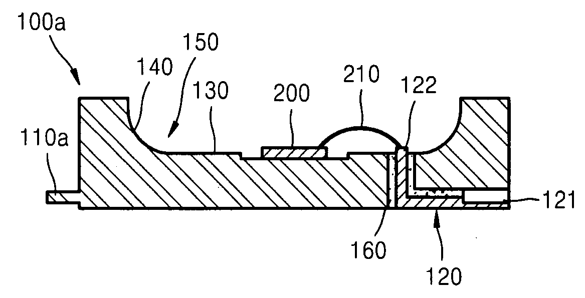
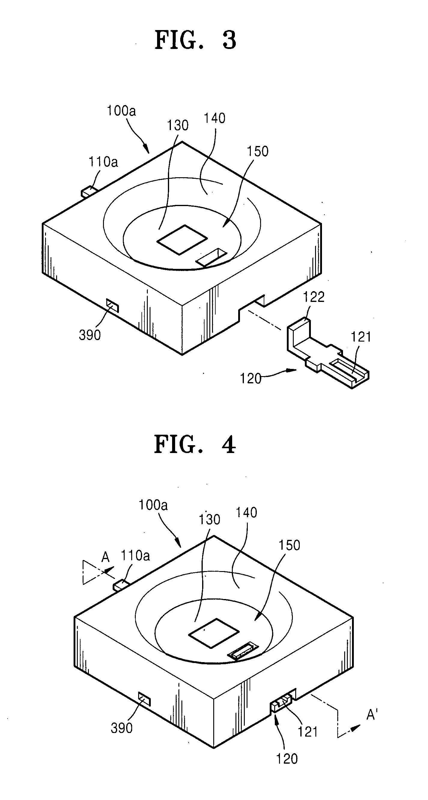
[0038]Detailed example embodiments are disclosed herein. However, specific structural and / or functional details disclosed herein are merely representative for purposes of describing example embodiments. The claims may, however, may be embodied in many alternate forms and should not be construed as limited to only example embodiments set forth herein.

[0039]It will be understood that when a component is referred to as being “on,”“connected to” or “coupled to” another component, it can be directly on, connected to or coupled to the other component or intervening components may be present. In contrast, when a component is referred to as being “directly on,”“directly connected to” or “directly coupled to” another component, there are no intervening components present. As used herein, the term “and / or” includes any and all combinations of one or more of the associated listed items.

[0040]It will be understood that, although the terms first, second, third, etc. may be used herein to describ...


PUM


Abstract

Example embodiments may include a light emitting device package. The light emitting device package may include a light emitting device, a package body including a cavity having a bottom surface on which the light emitting device is mounted and a side surface for reflecting light emitted from the light emitting device, a first electrode protruding from the package body, and a second electrode coupled with the package body. The first and second electrodes may be designed to couple respectively with the second and first electrodes of another light emitting device package, thereby forming an array of light emitting device packages.

Description

PRIORITY STATEMENT[0001]This application claims the benefit of Korean Patent Application No. 10-2006-0044640, filed on May 18, 2006, in the Korean Intellectual Property Office, the disclosure of which is incorporated herein in its entirety by reference.BACKGROUND[0002]1. Field[0003]Example embodiments relate to a light emitting device package and an array thereof, for example, to a light emitting device package array that may improve color uniformity and / or a package alignment of a light-emitting device package array.[0004]2. Description of the Related Art[0005]A related art light emitting device package may include a plurality of light emitting devices such as light emitting diodes (LED), a laser diode (LD), and / or a package body on which a light emitting device and electrodes may be mounted. A related-art light-emitting device package array may include a display device that displays letters or graphic images or a display lamp in which a plurality of light emitting device packages ...

Claims


Application Information

Patent Timeline
IPC IPC(8): H01L33/00H01L33/44H01L33/58H01L33/60H01L33/62
CPCH01L33/486H01L33/60H01L33/62H01L2224/48091H01L2924/09701H01L2924/01078H01L2924/00014
Inventor KIM, HYUNG-KUNKIM, YU-SIK
Owner SAMSUNG ELECTRONICS CO LTD
Why Eureka
Try Eureka