MOS devices with corner spacers

Inactive Publication Date: 2007-11-22
TAIWAN SEMICON MFG CO LTD
View PDF16 Cites 45 Cited by
  • Summary
  • Abstract
  • Description
  • Claims
  • Application Information

AI Technical Summary

Benefits of technology

[0013]The corner spacers space the silicide regions apart from the edge of the source/drain regions, thus reducing current crowding effects and

Problems solved by technology

Since significant portions of spacers are vertical, conventional single layer spacers suffer non-uniformity problems.
These problems are further worsened by the scaling of the integrated circuits.
However, when MOS devices are scaled down to 65 nm and below, they begin t

Method used


Image

  • MOS devices with corner spacers
  • MOS devices with corner spacers
  • MOS devices with corner spacers

Examples


Embodiment Construction

[0017]The making and using of the presently preferred embodiments are discussed in detail below. It should be appreciated, however, that the present invention provides many applicable inventive concepts that can be embodied in a wide variety of specific contexts. The specific embodiments discussed are merely illustrative of specific ways to make and use the invention, and do not limit the scope of the invention.

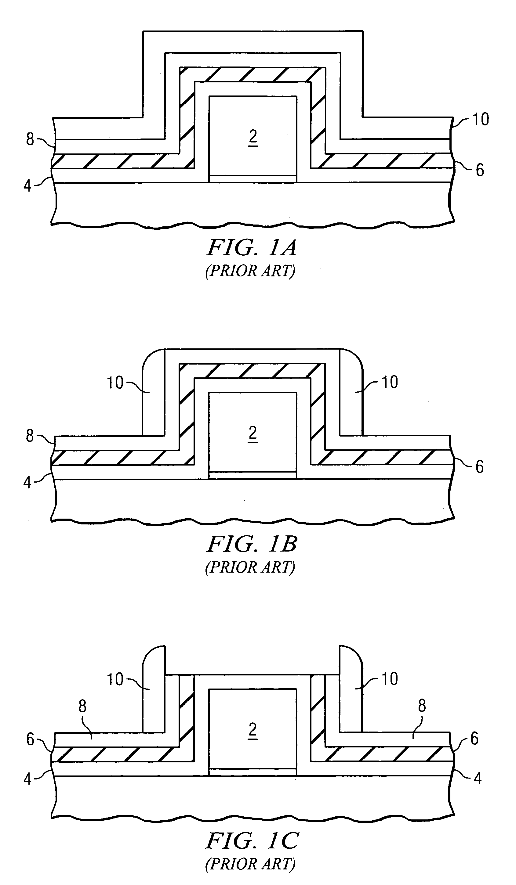
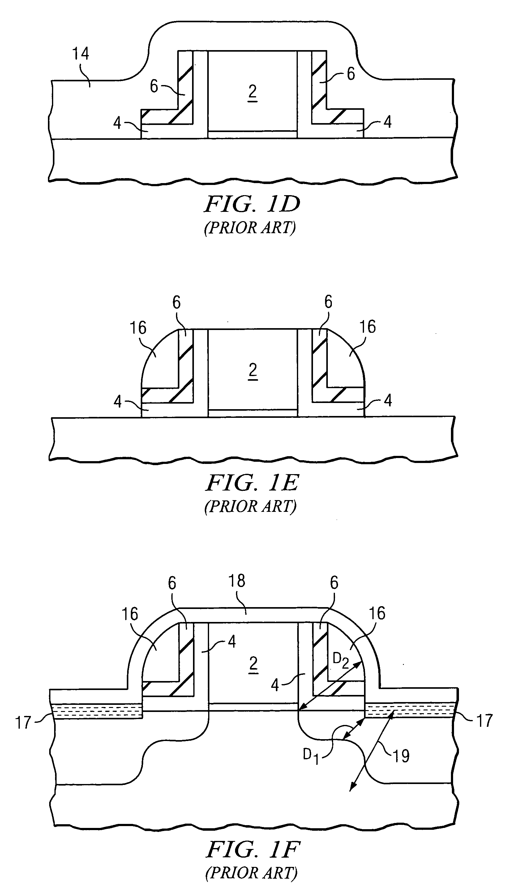
[0018]The intermediate stages of manufacturing a preferred embodiment of the present invention are illustrated. Variations of the preferred embodiment are then discussed. Throughout the various views and illustrative embodiments of the present invention, like reference numbers are used to designate like elements.

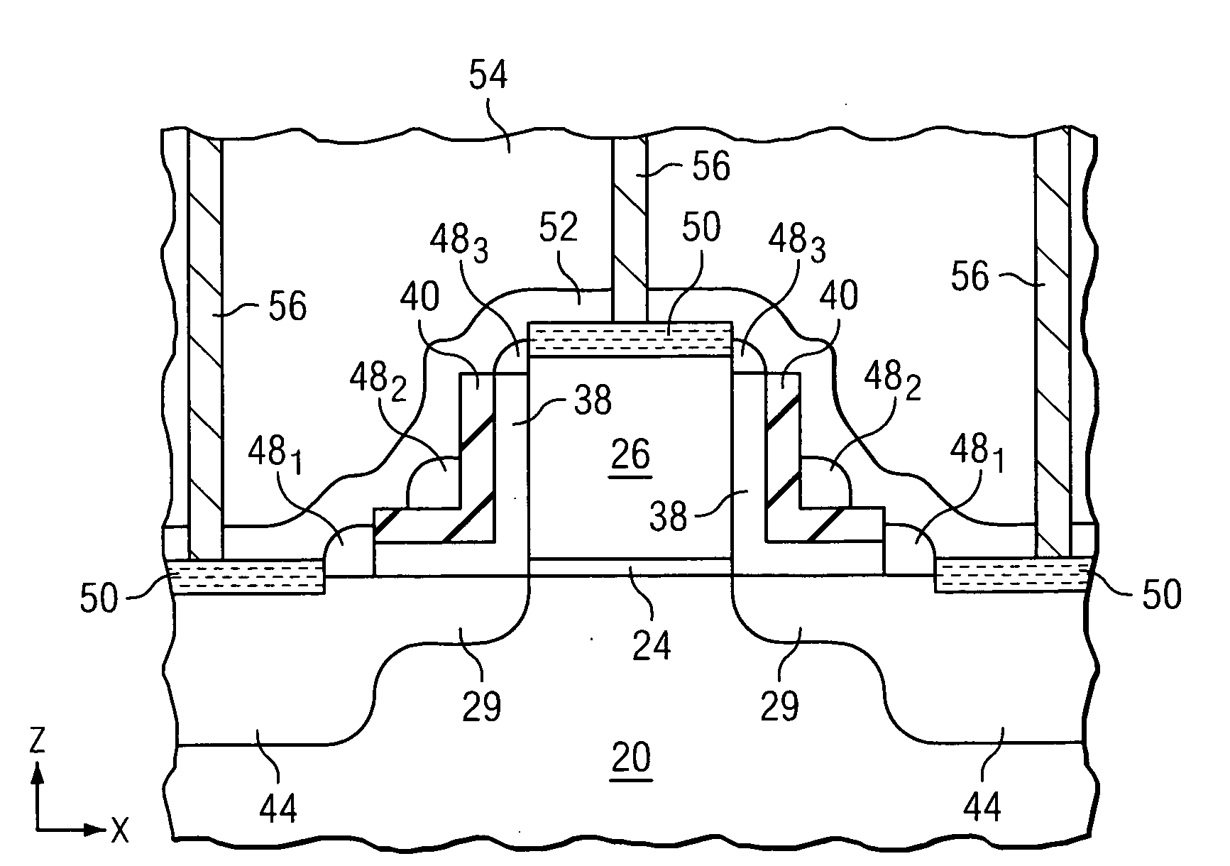
[0019]FIG. 2 illustrates a gate stack, which comprises a gate dielectric 24 and a gate electrode 26, formed on a substrate 20. Gate dielectric 24 preferably has a high dielectric constant (k value). Substrate 20 may be a bulk silicon substrate, although other commonly...


PUM


Abstract

A MOS device having corner spacers and a method for forming the same are provided. The method includes forming a gate structure overlying a substrate, forming a first dielectric layer over the gate structure and the substrate, forming a second dielectric layer on the first dielectric layer, forming a third dielectric layer on the second dielectric layer, and etching the first, the second and the third dielectric layers using the third dielectric layer as a mask. The remaining first and second dielectric layers have an L-shape. The method further includes implanting source/drain regions, removing remaining portions of the third dielectric layer, blanket forming a fourth dielectric layer, etching the fourth dielectric layer, siliciding exposed source/drain regions, and forming a contact etch stop layer. The remaining portion of the fourth dielectric layer forms corner spacers.

Description

TECHNICAL FIELD[0001]This invention relates generally to semiconductor devices, and more particularly to the structure and fabrication methods of MOS devices, and even more particularly to a method of forming spacers.BACKGROUND[0002]Spacers are key elements in modern metal-oxide-semiconductor (MOS) devices. They provide several key functions. Besides insulating gate electrodes and source / drain regions, they are also used as implant masks for implanting source and drain regions and forming silicide regions.[0003]Typically, spacers are formed by blanket depositing a dielectric layer after the formation of gate electrodes, forming and patterning a photo resist on the dielectric layer, and etching undesired portions of the dielectric layer. Remaining portions of the dielectric layer, typically including vertical portions on the sidewalls of the gate electrodes and possibly small horizontal portions adjacent the vertical portions, become spacers.[0004]Since significant portions of spacer...

Claims


Application Information

Patent Timeline
IPC IPC(8): H01L29/76
CPCH01L29/4983H01L29/665H01L29/7833H01L29/6656H01L29/6659H01L29/6653
Inventor LO, CHENG-YAO
Owner TAIWAN SEMICON MFG CO LTD
Why Eureka
Try Eureka