Metal/gallium nitride aluminum /gallium nitride lateral direction schottky diode with low current collection side effect and method of producing the same

A Schottky diode, aluminum gallium nitride technology, applied in semiconductor/solid-state device manufacturing, electrical components, circuits, etc., can solve the problem that the lateral Schottky diode current edge effect cannot be effectively alleviated, and it is difficult to reduce production costs. Increase the difficulty of production and other problems to achieve the effect of eliminating the possibility of failure or damage, reducing the current edge effect, and increasing efficiency

Inactive Publication Date: 2009-08-12
HEFEI INSTITUTES OF PHYSICAL SCIENCE - CHINESE ACAD OF SCI
View PDF4 Cites 0 Cited by
  • Summary
  • Abstract
  • Description
  • Claims
  • Application Information

AI Technical Summary

Problems solved by technology

To solve this problem, people will have to reduce the width of the anode of the lateral Schottky diode when designing the anode of the lateral Schottky diode, but this will greatly increase the difficulty of manufacture; secondly, this preparation method is both It cannot effectively alleviate the current collector effect of the lateral Schottky diode, and it is difficult to reduce the production cost due to the single process

Method used


Image

  • Metal/gallium nitride aluminum /gallium nitride lateral direction schottky diode with low current collection side effect and method of producing the same
  • Metal/gallium nitride aluminum /gallium nitride lateral direction schottky diode with low current collection side effect and method of producing the same
  • Metal/gallium nitride aluminum /gallium nitride lateral direction schottky diode with low current collection side effect and method of producing the same

Examples


Embodiment 1

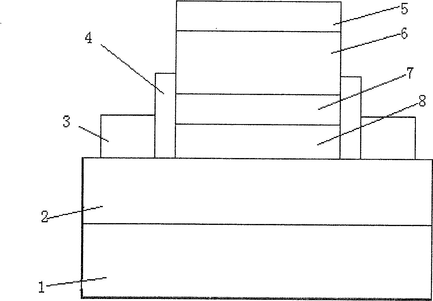
[0015] Embodiment 1: Complete the preparation in sequence according to the following steps: a) first use the epitaxial method to grow a gallium nitride layer on the substrate, wherein the substrate is selected from sapphire, and the epitaxial method is selected from the molecular beam epitaxy method, and the conditions during growth are the same as the existing . Then use the existing method to grow or deposit the positive electrode, the negative electrode and the mask respectively on the gallium nitride layer, wherein, the mask is deposited on the surface of the gallium nitride layer by using the plasma enhanced chemical vapor deposition method, depositing When the pressure is 1Pa, other conditions are the same as the existing ones, the mask is a silicon nitride mask; the negative electrode is deposited on the surface of the gallium nitride layer using the existing method, the negative electrode is an ohmic contact, and the contact layer is titanium aluminum alloy layer; the ...

Embodiment 2

[0016] Embodiment 2: Complete the preparation sequentially according to the following steps: a) first use epitaxy to grow a gallium nitride layer on the substrate, wherein the substrate is sapphire, and the epitaxy is molecular beam epitaxy. . Then use the existing method to grow or deposit the positive electrode, the negative electrode and the mask respectively on the gallium nitride layer, wherein, the mask is deposited on the surface of the gallium nitride layer by using the plasma enhanced chemical vapor deposition method, depositing When the pressure is 1.5Pa, other conditions are the same as the existing ones, the mask is a silicon nitride mask; the negative electrode is deposited on the surface of the gallium nitride layer using the existing method, the negative electrode is an ohmic contact, and the contact layer is titanium An aluminum alloy layer; an existing method is used to grow an aluminum gallium nitride layer on the surface of the gallium nitride layer; a tanta...

Embodiment 3

[0017] Embodiment 3: Complete the preparation sequentially according to the following steps: a) first use the epitaxy method to grow a gallium nitride layer on the substrate, wherein the substrate is sapphire, the epitaxy method is molecular beam epitaxy, and the growth conditions are the same as the existing . Then use the existing method to grow or deposit the positive electrode, the negative electrode and the mask respectively on the gallium nitride layer, wherein, the mask is deposited on the surface of the gallium nitride layer by using the plasma enhanced chemical vapor deposition method, depositing When the pressure is 2Pa, other conditions are the same as the existing ones, the mask is a silicon nitride mask; the negative electrode is deposited on the surface of the gallium nitride layer using the existing method, the negative electrode is an ohmic contact, and the contact layer is titanium aluminum alloy layer; the existing method is used to grow the aluminum gallium ...


PUM

PropertyMeasurementUnit
thicknessaaaaaaaaaa
thicknessaaaaaaaaaa
thicknessaaaaaaaaaa

Abstract

The invention discloses a metal / gallium aluminum nitride / gallium nitride lateral schottky diode with low current edge collection effect and a preparation method thereof. The diode has a gallium nitride layer (2), a positive electrode, a negative electrode (3) and a mask (4) on a substrate (1), the positive electrode contains a gallium nitride aluminum layer (8), and a Schottky contact metal layer (7) , a polysilicon layer (6) and a metal electrode layer (5); the method is (a) first growing a gallium nitride layer on a substrate by epitaxial method, and then growing or depositing a positive electrode and a negative electrode respectively on it using an existing method and mask; (b) using low-pressure chemical vapor deposition or metal sputtering or electron cyclotron resonance-plasma enhanced chemical vapor deposition to deposit a polysilicon layer on the Schottky contact metal layer, while using ion implantation or Diffusion method or doping method in chemical vapor deposition is used to adjust the resistivity of the polysilicon layer to obtain the diode of the present invention. The current distribution at the edge of its positive electrode is uniform, which is very suitable for high temperature and high power devices.

Description

technical field [0001] The invention relates to a Schottky diode and a manufacturing method thereof, in particular to a metal / gallium aluminum nitride / gallium nitride lateral Schottky diode and a preparation method thereof. Background technique [0002] Gallium nitride (GaN) is the most widely used semiconductor material after the second-generation semiconductor materials gallium arsenide (GaAs) and indium phosphide (InP). GaN is especially suitable for high-temperature and high-power devices because of its wide band gap, high critical breakdown field strength, good electron transport characteristics and thermal conductivity characteristics. Aluminum gallium nitride (AlGaN) materials have the same lattice structure as GaN materials, and the lattice mismatch with GaN does not exceed 2.5%, making it possible to realize AlGaN / GaN heterojunction devices. At present, devices centered on AlGaN / GaN heterojunctions are increasingly developed, including metal / AlGaN / GaN heterojunctio...

Claims


Application Information

Patent Timeline
Patent Type & Authority Patents(China)
IPC IPC(8): H01L29/872H01L21/329
Inventor 陈家荣王玉琦陈文锦邱凯李新化
Owner HEFEI INSTITUTES OF PHYSICAL SCIENCE - CHINESE ACAD OF SCI
Why Eureka
Try Eureka