MicroLED chip and manufacturing method thereof

A manufacturing method and chip technology, applied to semiconductor devices, electrical components, circuits, etc., can solve problems such as chip efficiency reduction, life shortening, device failure, etc., and achieve the effects of distribution optimization, effective resistance reduction, and high specific surface area

Active Publication Date: 2022-04-19
WUHAN UNIV
View PDF4 Cites 0 Cited by
  • Summary
  • Abstract
  • Description
  • Claims
  • Application Information

AI Technical Summary

Problems solved by technology

[0004] By providing a MicroLED chip and a manufacturing method thereof, the present invention solves the problems in the prior art that the heat accumulation of the MicroLED chip is relatively serious, resulting in reduced chip efficiency, shortened lifespan, and device failure.

Method used


Image

  • MicroLED chip and manufacturing method thereof
  • MicroLED chip and manufacturing method thereof
  • MicroLED chip and manufacturing method thereof

Examples


Embodiment 1

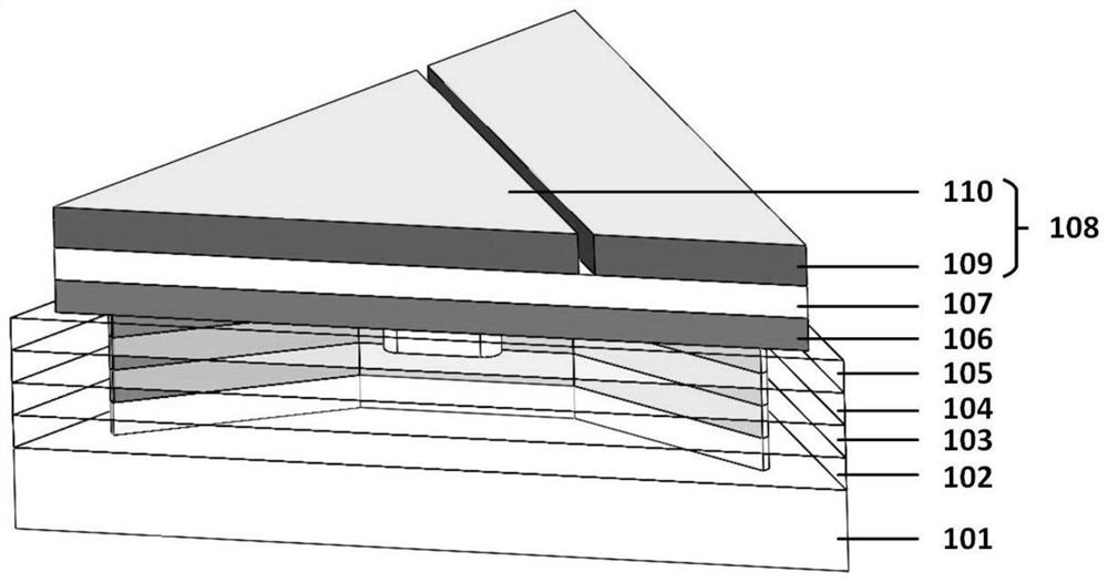
[0045] Embodiment 1 provides a method for manufacturing a MicroLED chip, see figure 1 , including the following steps:

[0046] Step 1, growing the epitaxial layer of the Micro LED chip on the growth substrate, the epitaxial layer includes an n-type semiconductor layer, a multi-quantum well layer and a p-type semiconductor layer in sequence from bottom to top.

[0047] Specifically, see figure 1 , figure 2 The epitaxial layer 202 is grown on a sapphire substrate by MOCVD method, and the epitaxial layer 202 includes a 2-4 μm n-GaN layer 101, 5-12 pairs of InGaN / GaN multiple quantum well layers 102 and 80 from bottom to top - 300nm Mg-doped p-GaN layer 103; in each InGaN / GaN pair, the thickness of InGaN is 1-3nm, and the thickness of GaN is 8-15nm.

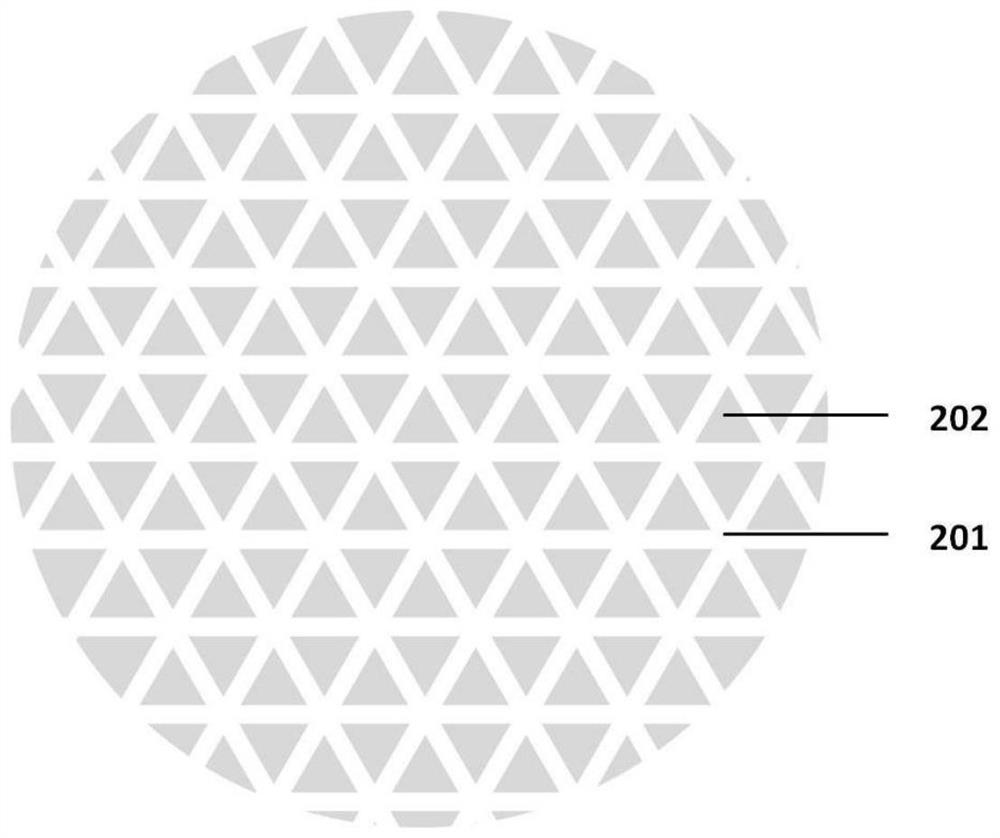
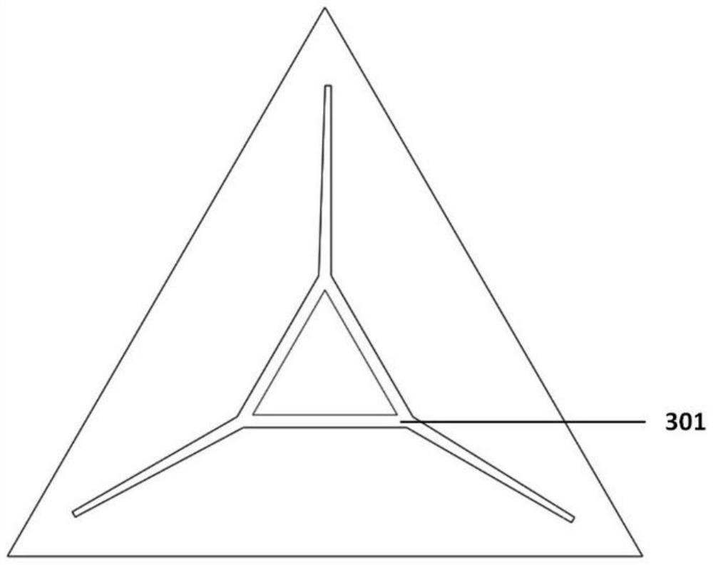
[0048] Step 2, etching chip isolation trenches on the epitaxial layer, and forming an epitaxial layer including a plurality of mesa regions in a triangular shape after the etching is completed.

[0049] Specifically, such as ...

Embodiment 2

[0067] Embodiment 2 provides a Micro LED chip, which is prepared by using the manufacturing method of the Micro LED chip provided in Embodiment 1.

[0068] see Figure 1 to Figure 6 , the chip structure of the Micro LED chip is a thin-film flip-chip structure, and the shape of the Micro LED chip is a triangle.

[0069] The growth substrate of the Micro LED chip is a sapphire substrate, and after the chip is manufactured, the sapphire growth substrate is peeled off. The epitaxial layer grown on the sapphire substrate is an n-type semiconductor layer, a multi-quantum well layer, and a p-type semiconductor layer in sequence from bottom to top. The epitaxial layer is etched into a triangular-shaped structure including a plurality of mesa regions.

[0070] Specifically, the epitaxial layer 202 of the Micro LED chip is an n-GaN layer 101 , an InGaN / GaN multiple quantum well layer 102 and a p-GaN layer 103 in sequence.

[0071] On the p-GaN layer 103 is an ITO layer 104 , the ITO ...


PUM

PropertyMeasurementUnit
thicknessaaaaaaaaaa
thicknessaaaaaaaaaa

Abstract

The invention belongs to the technical field of display, and discloses a MicroLED chip and a manufacturing method thereof. The MicroLED chip provided by the invention is in a triangular shape, is of a thin film inverted structure, comprises the patterned double-layer metal electrode, and has a higher specific surface area compared with a conventional chip structure, the distribution of the n-type electrode is optimized, the current aggregation effect near the n-type electrode can be effectively reduced, the effective resistance of the n-type semiconductor layer is reduced, and the service life of the micro LED chip is prolonged. And the heat accumulation effect of the chip can be obviously improved.

Description

technical field [0001] The invention belongs to the field of display technology, and more specifically relates to a Micro LED chip and a manufacturing method thereof. Background technique [0002] Micro LED refers to a micro LED (Light Emitting Diode, light emitting diode) with a device width of less than 50 μm. In the display technology based on MicroLED chips, each MicroLED is equivalent to a pixel, and the pixel pitch is reduced to the micron level, and each pixel can be individually addressed and lit. Compared with traditional display technologies such as LCD and OLED, the display technology based on Micro-LED chips has the advantages of low power consumption, high brightness, high efficiency, short response time, long life, ultra-high resolution and color saturation. It has obvious advantages and has important application value in the fields of high-resolution display, helmet display, augmented reality, micro-projector and wearable electronics. [0003] Compared with ...

Claims


Application Information

Patent Timeline
Patent Type & Authority Applications(China)
IPC IPC(8): H01L33/00H01L33/20H01L33/38
CPCH01L33/007H01L33/20H01L33/38H01L2933/0016
Inventor 周圣军雷宇
Owner WUHAN UNIV
Why Eureka
Try Eureka