Semiconductor MPS diode with reduced current-crowding effect and manufacturing method thereof

a technology of mps diodes and current-crowding effect, which is applied in the direction of diodes, semiconductor devices, electrical apparatus, etc., can solve the problems of failure of mps devices, failure of devices or thermomechanical devices, and cracks in dies, so as to reduce current-crowding

Active Publication Date: 2022-08-16
STMICROELECTRONICS SRL
View PDF9 Cites 0 Cited by
  • Summary
  • Abstract
  • Description
  • Claims
  • Application Information

AI Technical Summary

Benefits of technology

[0013]One or more embodiments of the present disclosure provide a MPS diode with reduced current-crowding effect and a manufacturing method thereof, to overcome the drawbacks of the prior art.

Problems solved by technology

Thermal runaway on very limited regions, even at relatively small currents, causes the formation of hot spots having a temperature that reaches high values, up to the material melting point, thus inducing a failure of the device or thermo-mechanical stresses that may ultimately lead to cracks in the die.
Even though the cell-like layouts of the solutions of FIGS. 2 and 3 allow to avoid current crowding at device corners, the present Applicant found that a small local imbalance of current or temperature of one of the JB elements 9 or Schottky diodes 12 may lead to a local electro-thermal runaway which may cause a failure of the MPS device.
Moreover, the presence of several bipolar cells, even if provided with dedicated ohmic contacts 9″, does not ensure a fast spreading of bipolar conduction current over the whole PN junction surface.

Method used


Image

  • Semiconductor MPS diode with reduced current-crowding effect and manufacturing method thereof
  • Semiconductor MPS diode with reduced current-crowding effect and manufacturing method thereof
  • Semiconductor MPS diode with reduced current-crowding effect and manufacturing method thereof

Examples


Embodiment Construction

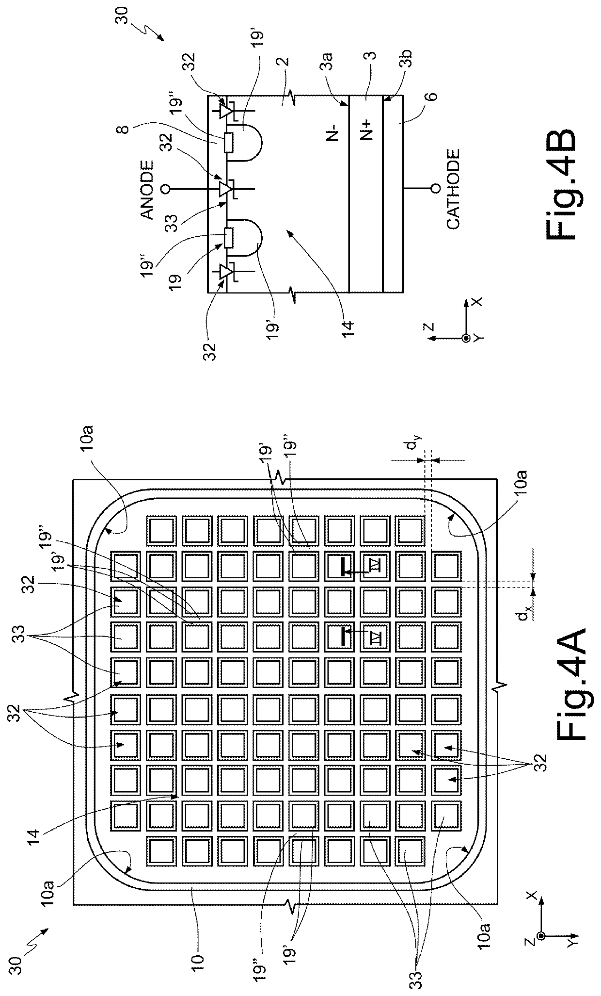
[0024]FIG. 4A shows, in the same reference system of axis X, Y, Z of FIGS. 1A-3, a top-plan view (i.e., on XY plane) of a Merged-PN-Schottky (MPS) device 30 (in particular, a MPS diode), according to an embodiment of the present invention. FIG. 4B shows, in the same reference system, a lateral sectional view taken along line IV-IV of FIG. 4A. To improve the understanding of FIG. 4A, the anode metallization 8 is not shown, even if present, as apparent from the view of FIG. 4B.

[0025]The lateral sectional view (i.e., on XZ plane) of FIG. 4B conforms substantially to that of FIG. 1B. Analogous elements are identified with the same reference numerals and not further described in detail.

[0026]However, when considering the top-plan view of FIG. 4A, the skilled person can appreciate that each Schottky diode 32 of a plurality of Schottky diodes 32 includes a respective Schottky cell (or dot) 33 having, in top-plan view on XY plane, a squared shape; the Schottky cells 33 are arranged in a gri...


PUM

PropertyMeasurementUnit
forbidden band gapaaaaaaaaaa
resistivityaaaaaaaaaa

Abstract

A merged-PN-Schottky, MPS, diode includes an N substrate, an N-drift layer, a P-doped region in the drift layer, an ohmic contact on the P-doped region, a plurality of cells within the P-doped region and being portions of the drift layer where the P-doped region is absent, an anode metallization on the ohmic contact and on said cells, to form junction-barrier contacts and Schottky contacts respectively. The P-doped region has a grid-shaped layout separating from one another each cell and defining, together with the cells, an active area of the MPS diode. Each cell has a same geometry among quadrangular, quadrangular with rounded corners and circular; and the ohmic contact extends at the doped region with continuity along the grid-shaped layout.

Description

BACKGROUNDTechnical Field[0001]The present disclosure relates to a semiconductor merged-PN-Schottky (MPS) diode with reduced current-crowding effect and a manufacturing method thereof.Description of the Related Art[0002]As is known, semiconductor materials which have a wide forbidden band gap, in particular, which have an energy value Eg of the forbidden band gap greater than 1.1 eV, low on-state resistance (RON), high value of thermal conductivity, high operating frequency, and high velocity saturation of charge carriers, are ideal for producing electronic components, such as diodes or transistors, in particular for power applications. A material having said characteristics, and designed to be used manufacturing electronic components, is silicon carbide (SiC). In particular, silicon carbide, in its different polytypes (e.g., 3C—SiC, 4H—SiC, 6H—SiC), is preferable to silicon as regards the properties listed previously.[0003]Electronic devices provided on a silicon carbide substrate,...

Claims


Application Information

Patent Timeline
Patent Type & Authority Patents(United States)
IPC IPC(8): H01L29/45H01L29/872H01L29/06H01L29/16H01L29/20H01L29/47H01L29/66
CPCH01L29/872H01L29/0619H01L29/1608H01L29/2003H01L29/45H01L29/47H01L29/66143H01L29/66212H01L29/0665H01L29/0692H01L29/6606
Inventor RASCUNA′, SIMONESAGGIO, MARIO GIUSEPPE
Owner STMICROELECTRONICS SRL
Why Eureka
Try Eureka