
Semiconductor device with a distributed plating pattern

a semiconductor and distributed plating technology, applied in the direction of printed circuit stress/warp reduction, non-metallic protective coating application, printed circuit aspects, etc., can solve the problems of electrically testing the trace pattern in the substrate before connecting the die thereto, noise, and electrical so as to reduce the mechanical stress on the semiconductor die

Inactive Publication Date: 2007-11-22
SANDISK TECH LLC
View PDF9 Cites 7 Cited by
  • Summary
  • Abstract
  • Description
  • Claims
  • Application Information

AI Technical Summary

Benefits of technology

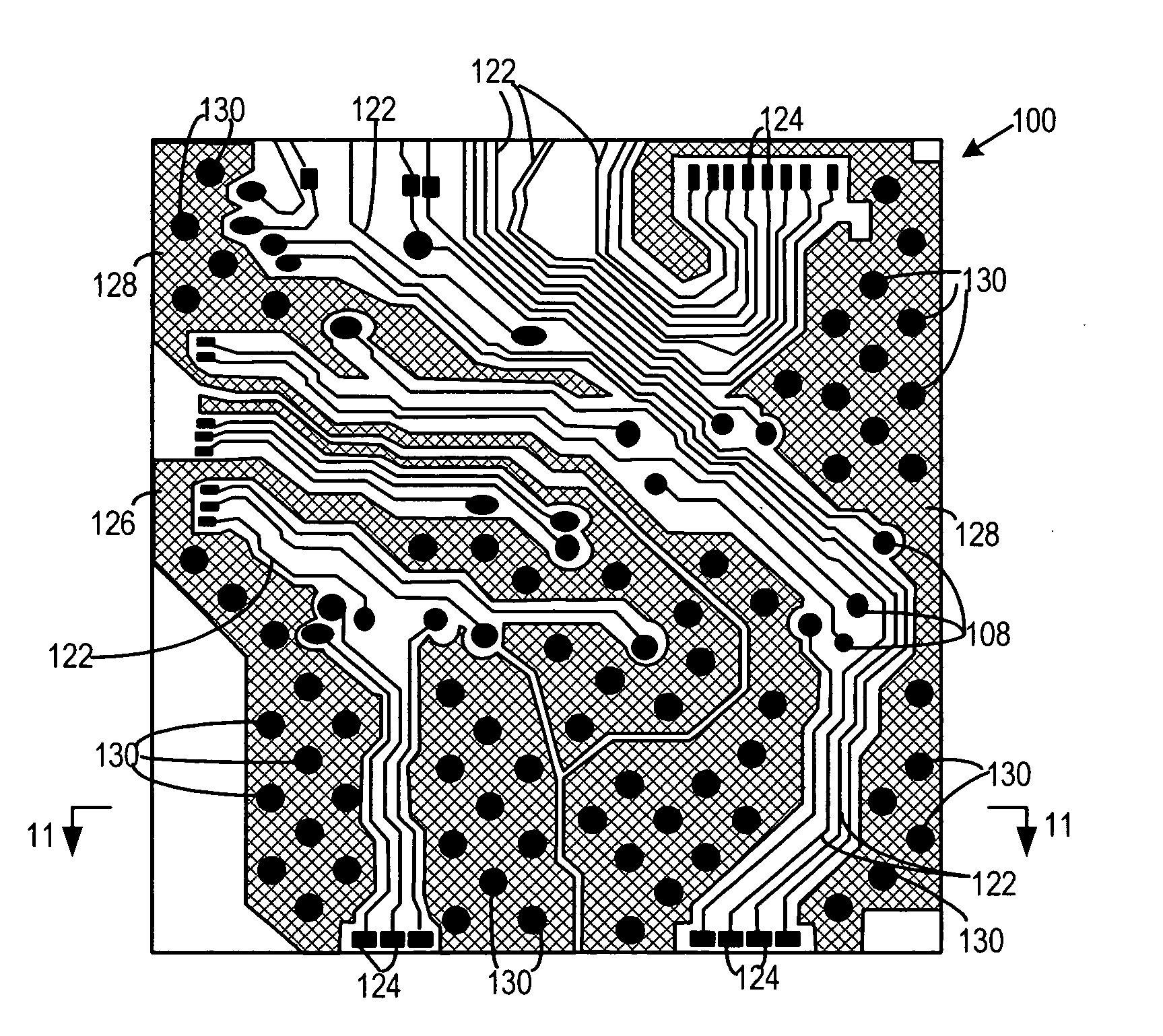
[0013]Embodiments of the invention relate to a substrate, and a semiconductor die package formed therefrom, including a distributed plating pattern for reducing mechanical stress on the semiconductor die. The substrate according to embodiments of the invention may include traces and contact pads plated in a double image plating process. Additionally, the substrate may include areas, referred to herein as dummy plating areas, which also include plating.
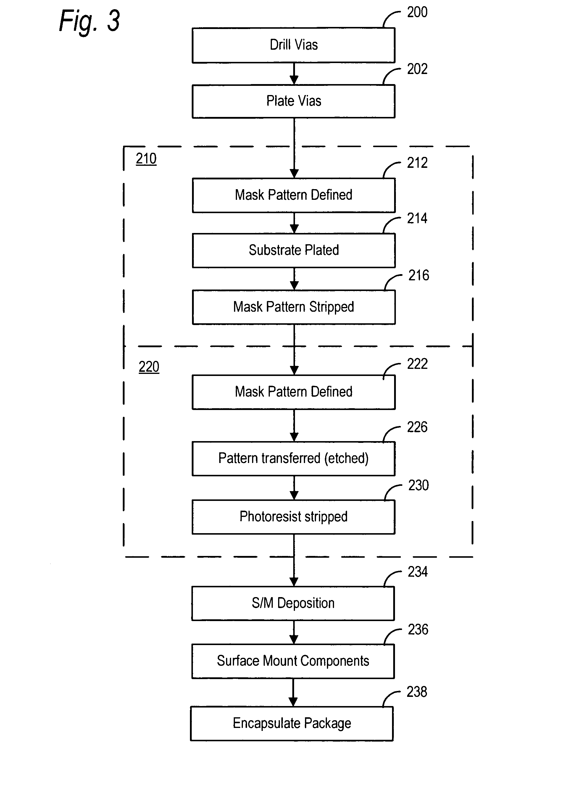
[0014]The substrate in embodiments of the invention may be fabricated in a double image process to include vias, plated electrical traces, plated contact pads, plated contact fingers, dummy patterns and the dummy plating areas. The plating material in the dummy plating areas serves to increase the amount of plating on the surface of the substrate, thereby lessening the space between adjacent plated vias or leads found in conventional substrates. The plated vias and / or traces and the plating within the dummy plating areas provide a plating pattern which is evenly distributed across the surface of the substrate. The even distribution of the plating pattern prevents peaks and valleys in the finished substrate.

Problems solved by technology

While an efficient method for plating electrical contacts on substrates, electroplating has drawbacks.
First, the electrical connections between all contacts often are not severed until package singulation, making it impossible to electrically test the trace pattern in the substrate before connecting the die thereto.
Moreover, the large area of the plating tails takes up valuable real estate on the substrate, and also may create noise due to the antenna effect.
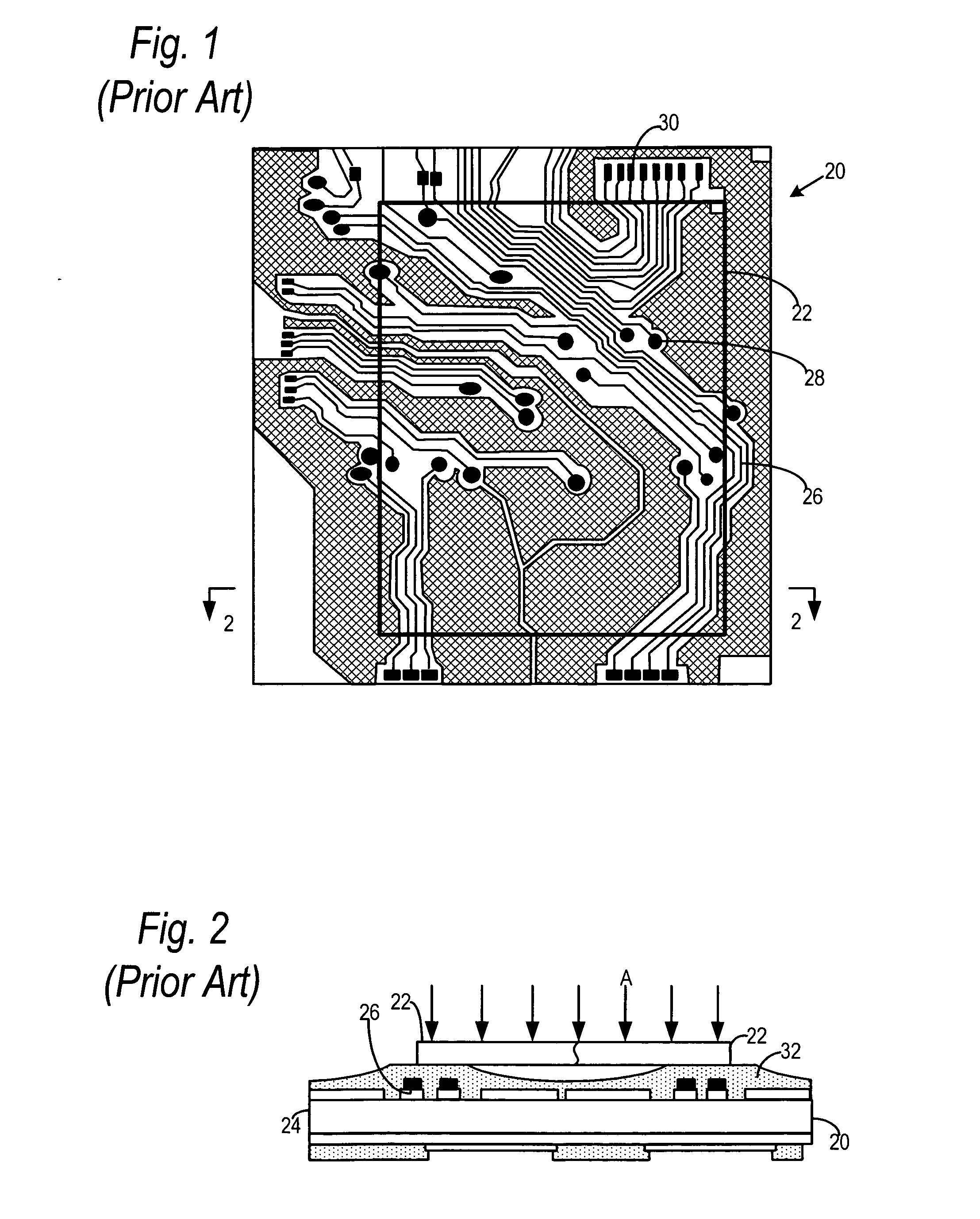
A problem with conventional substrates formed by double image processing is that the surface of the substrate is not flat.
However, the constant drive toward smaller form factor packages require very thin die.
At these thicknesses, the die are often not able to withstand the stresses generated during the molding process and they may crack.
Die cracking under the stress of the molding process will generally result in the package having to be discarded.
Occurring at the end of the semiconductor fabrication and packaging process, this is an especially costly and burdensome problem.

Method used


Image

  • Semiconductor device with a distributed plating pattern
  • Semiconductor device with a distributed plating pattern
  • Semiconductor device with a distributed plating pattern

Examples


Embodiment Construction

[0034]Embodiments of the invention are described with reference to FIGS. 3 through 17, which relate to a substrate, and a semiconductor die package formed therefrom, including a distributed plating pattern for reducing mechanical stress on the semiconductor die. It is understood that the present invention may be embodied in many different forms and should not be construed as being limited to the embodiments set forth herein. Rather, these embodiments are provided so that this disclosure will be thorough and complete and will fully convey the invention to those skilled in the art. Indeed, the invention is intended to cover alternatives, modifications and equivalents of these embodiments, which are included within the scope and spirit of the invention as defined by the appended claims. Furthermore, in the following detailed description of the present invention, numerous specific details are set forth in order to provide a thorough understanding of the present invention. However, it wi...


PUM


Abstract

A substrate, and a semiconductor die package formed therefrom, are disclosed which include a distributed plating pattern for reducing mechanical stress on the semiconductor die. The substrate according to embodiments of the invention may include traces and contact pads plated in a double image plating process. Additionally, the substrate may include dummy plating areas including plating material. The plated vias and / or traces and the plating material within the dummy plating areas provide a plating pattern which is evenly distributed across the surface of the substrate. The even distribution of the plating pattern prevents peaks and valleys in the finished substrate.

Description

CROSS REFERENCE TO RELATED APPLICATION[0001]This application is related to United States Patent Application entitled “METHOD OF REDUCING STRESS ON A SEMICONDUCTOR DIE WITH A DISTRIBUTED PLATING PATTERN”, Inventors Chih-Chin Liao, Han-Shiao Chen, Chin-Tien Chiu, Cheemen Yu, Hem Takiar, filed on the same day as the present application and incorporated herein by reference in its entirety.BACKGROUND OF THE INVENTION[0002]1. Field of the Invention[0003]Embodiments of the present invention relate to a substrate, and a semiconductor die package formed therefrom, including a distributed plating pattern for reducing mechanical stress on the semiconductor die.[0004]2. Description of the Related Art[0005]The strong growth in demand for portable consumer electronics is driving the need for high-capacity storage devices. Non-volatile semiconductor memory devices, such as flash memory storage cards, are becoming widely used to meet the ever-growing demands on digital information storage and excha...

Claims


Application Information

Patent Timeline
Patent Type & Authority Applications(United States)
IPC IPC(8): H01L23/48
CPCH01L23/49838H05K1/0271H05K3/243H05K3/28H05K2201/09781H01L2924/0002H05K2201/0989H01L2924/00
Inventor LIAO, CHIH-CHINCHEN, HAN-SHIAOCHIU, CHIN-TIENYU, CHEEMENTAKIAR, HEM
Owner SANDISK TECH LLC
Features
  • Generate Ideas
  • Intellectual Property
  • Life Sciences
  • Materials
  • Tech Scout
  • Unparalleled Data Quality
  • Higher Quality Content
  • 60% Fewer Hallucinations
Learn More