Semiconductor wafer handling and transport

a technology of semiconductor wafers and wafers, applied in the direction of transportation and packaging, conveyors, packaging goods types, etc., can solve the problems of large space occupation, linear tools, cluster tools, and offer much greater flexibility and the potential for greater speed than cluster tools, and achieve convenient manufacturing methods, facilitate proper vacuum sealing, and small footprint

Inactive Publication Date: 2007-11-22
BLUESHIFT TECH +2
View PDF0 Cites 88 Cited by
  • Summary
  • Abstract
  • Description
  • Claims
  • Application Information

AI Technical Summary

Benefits of technology

[0010] Provided herein are methods and systems used for improved semiconductor manufacturing handling, and transport. Modular wafer transport and handling facilities are combined in a variety of ways deliver greater levels of flexibility, utility, efficiency, and functionality in a vacuum semiconductor processing system. Various processing and other modules may be interconnected with tunnel-and-cart transportation systems to extend the distance and versatility of the vacuum environment. Other improvements such as bypass thermal adjusters, buffering aligners, batch processing, multifunction modules, low particle vents, cluster processing cells, and the like are incorporated to expand functionality and improve processing efficiency.
[0027] As used herein, the term “SCARA arm” refers to a robotic arm that includes one or more links and may include an end effector, where the arm, under control, can move linearly, such as to engage an object. A SCARA arm may have various numbers of links, such as 3, 4, or more. As used herein, “3-link SCARA arm” shall include a SCARA robotic arm that has three members: link one (L1), link two (L2) and an end effector. A drive for a 3-link SCARA arm usually has 3 motors: one connected to L1, one to the belt system, which in turn connects to the end effector through pulleys and a Z (lift) motor. One can connect a fourth motor to the end effector, which allows for some unusual moves not possible with only three motors.
[0036] Disclosed herein are methods and systems for supporting vacuum processing and handling modules in vacuum semiconductor processing systems. The pedestal support systems herein disclosed may precisely position vacuum modules to facilitate proper vacuum sealing between adjacent modules. In embodiments, the pedestal's cylindrical shape affords opportunity for convenient manufacturing methods while providing stability to the supported vacuum module with a small footprint.
[0037] In embodiments, the pedestal support system further may incorporate a robot motor mechanism for a robot operating within the vacuum module, further reducing the overall size and cost of the vacuum processing system.
[0038] A pedestal support system with a rolling base may also provide needed flexibility in reconfiguring processing and handling modules quickly and cost effectively.

Problems solved by technology

Cluster tools, machines that arrange a group of semiconductor processing modules in a radius about a central robotic arm, take up a large amount of space, are relatively slow, and, by virtue of their architecture, are limited to a small number of semiconductor process modules, typically a maximum of about five or six.
Linear tools, while offering much greater flexibility and the potential for greater speed than cluster tools, do not fit well with the current infrastructure of most current semiconductor fabrication facilities.
Moreover, linear motion of equipment components within the typical vacuum environment of semiconductor manufacturing leads to problems in current linear systems, such as unacceptable levels of particles that are generated by friction among components.
As semiconductor manufacturing has grown in complexity, it becomes increasingly necessary to transfer wafers among a number of different process modules or clusters of process modules, and sometimes between tools and modules that are separated by significant distances.
This poses numerous difficulties, particularly when wafers are transferred between separate vacuum processing facilities.
Transfers between vacuum environments, or between a vacuum and other processing environments often results in increased risk of particle contamination (due to the pumping and venting of wafers in load locks) as well as higher thermal budgets where wafers are either heated or cooled during transfers.

Method used


Image

  • Semiconductor wafer handling and transport
  • Semiconductor wafer handling and transport
  • Semiconductor wafer handling and transport

Examples


Embodiment Construction

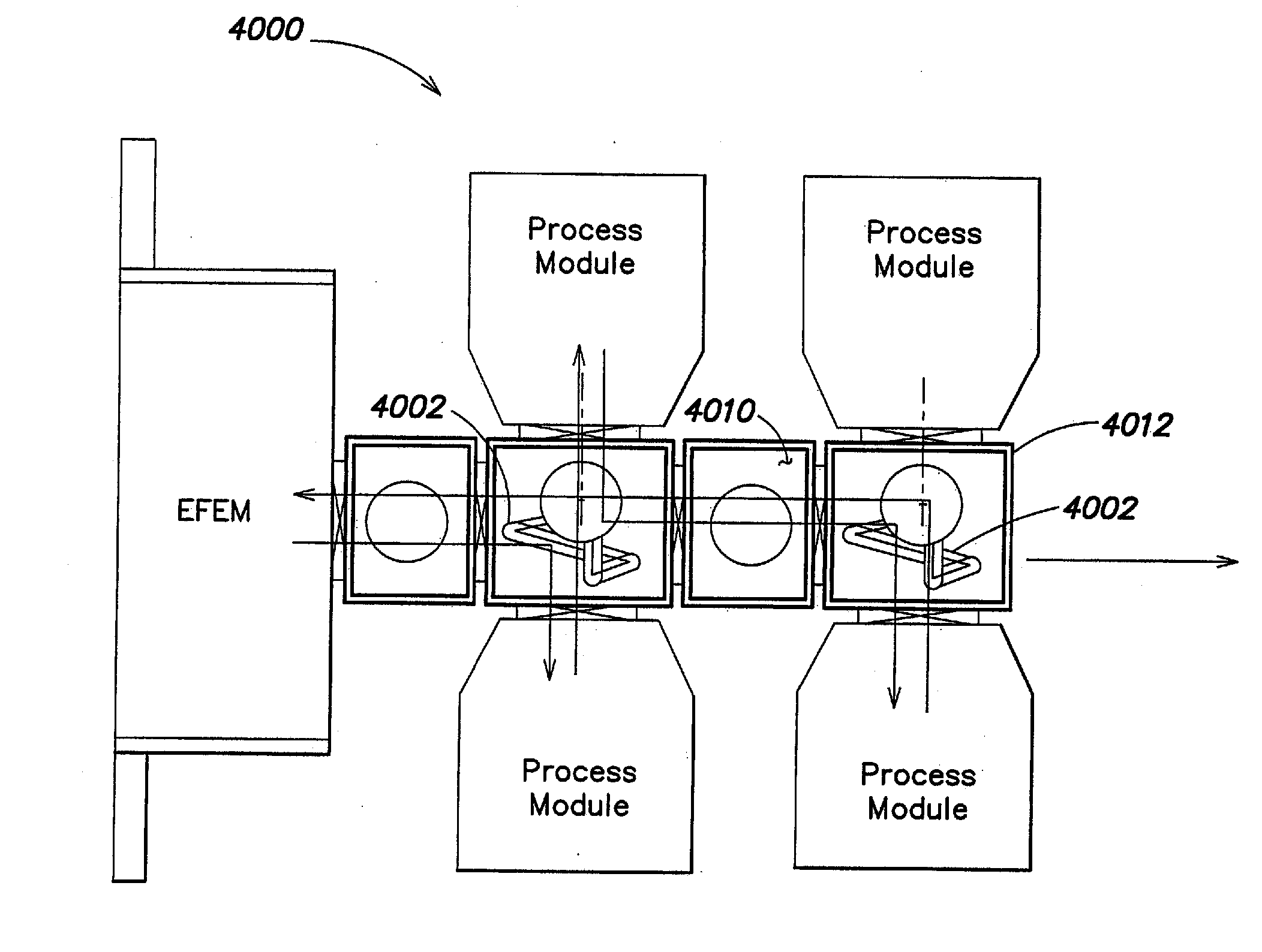
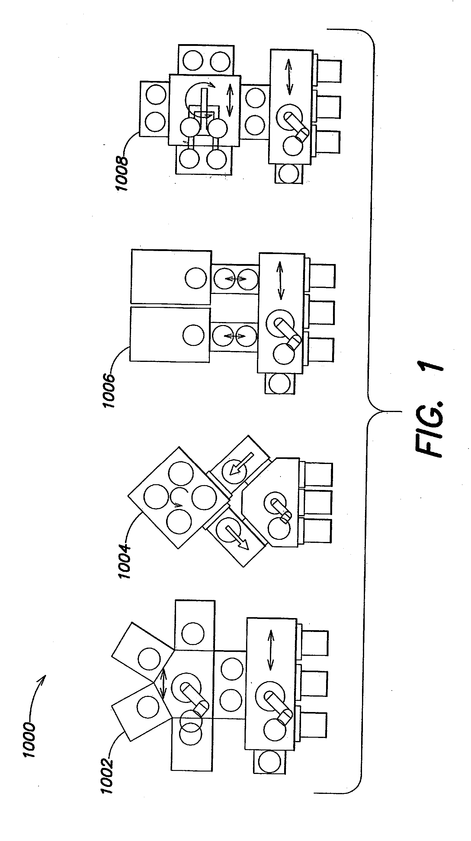
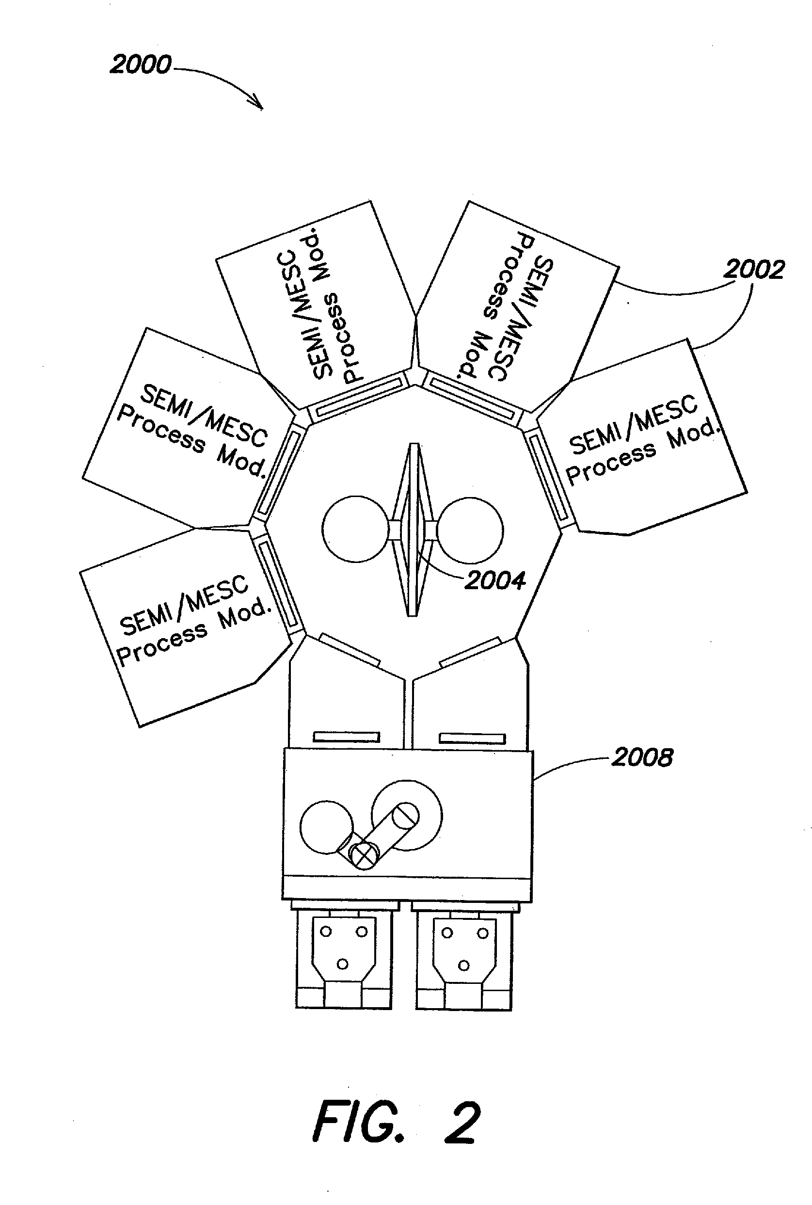
[0150]FIG. 1 shows equipment architectures 1000 for a variety of manufacturing equipment types. Each type of manufacturing equipment handles items, such as semiconductor wafers, between various processes, such as chemical vapor deposition processes, etching processes, and the like. As semiconductor manufacturing processes are typically extremely sensitive to contaminants, such as particulates and volatile organic compounds, the processes typically take place in a vacuum environment, in one or more process modules that are devoted to specific processes. Semiconductor wafers are moved by a handling system among the various processes to produce the end product, such as a chip. Various configurations 1000 exist for handling systems. A prevalent system is a cluster tool 1002, where process modules are positioned radially around a central handling system, such as a robotic arm. In other embodiments, a handling system can rotate items horizontally, such as in the embodiment 1004. An import...


PUM


Abstract

Modular wafer transport and handling facilities are combined in a variety of ways deliver greater levels of flexibility, utility, efficiency, and functionality in a vacuum semiconductor processing system. Various processing and other modules may be interconnected with tunnel-and-cart transportation systems to extend the distance and versatility of the vacuum environment. Other improvements such as bypass thermal adjusters, buffering aligners, batch processing, multifunction modules, low particle vents, cluster processing cells, and the like are incorporated to expand functionality and improve processing efficiency.

Description

RELATED APPLICATIONS [0001] This application is a continuation-in-part of U.S. application Ser. No. 10 / 985,834 filed on Nov. 10, 2004 which claims the benefit of U.S. Prov. App. No. 60 / 518,823 filed on Nov. 10, 2003 and U.S. Prov. App. No. 60 / 607,649 filed on Sep. 7, 2004. [0002] This application claims the benefit of U.S. Prov. App. No. 60 / 777,443 filed on Feb. 27, 2006; U.S. Prov. App. No. 60 / 779,684 filed on Mar. 5, 2006; U.S. Prov. App. No. 60 / 779,707 filed on Mar. 5, 2006; U.S. Prov. App. No. 60 / 779,478 filed on Mar. 5, 2006; U.S. Prov. App. No. 60 / 779,463 filed on Mar. 5, 2006; U.S. Prov. App. No. 60 / 779,609 filed on Mar. 5, 2006; U.S. Prov. App. No. 60 / 784,832 filed on Mar. 21, 2006; U.S. Prov. App. No. 60 / 746,163 filed on May 1, 2006; U.S. Prov. App. No. 60 / 807,189 filed on Jul. 12, 2006; and U.S. Prov. App. No. 60 / 823,454 filed on Aug. 24, 2006. [0003] The entire contents of each of the foregoing applications is incorporated herein by reference.BACKGROUND [0004] 1. Field of...

Claims


Application Information

Patent Timeline
Patent Type & Authority Applications(United States)
IPC IPC(8): B65G65/00
CPCB65G25/02B65G37/00H01L21/67161H01L21/67196H01L21/677H01L21/67745H01L21/67748H01L21/68792Y10S414/139H01L21/67742
Inventor MEULEN, PETER VAN DERKILEY, CHRISTOPHER C.PANNESE, PATRICK D.RITTER, RAYMOND S.SCHAEFER, THOMAS A.
Owner BLUESHIFT TECH
Why Eureka
Try Eureka