
Semiconductor wafer handling and transport

a technology of semiconductor wafers and wafers, applied in the direction of conveyers, storage devices, electrical devices, etc., can solve the problems of large space occupation, linear tools, cluster tools, and offer much greater flexibility and the potential for greater speed than cluster tools, and achieve convenient manufacturing methods, facilitate proper vacuum sealing, and small footprint

Active Publication Date: 2014-09-18
BOOKS AUTOMATION US LLC
View PDF1 Cites 47 Cited by
  • Summary
  • Abstract
  • Description
  • Claims
  • Application Information

AI Technical Summary

Benefits of technology

The patent describes an improved semiconductor manufacturing system that uses modular facilities for transport and handling. This system offers greater flexibility, efficiency, and functionality by combining various processing and other modules. The system also includes a vacuum environment through interconnections with tunnel-and-cart transportation systems. Other improvements include bypass thermal adjusters, buffering aligners, batch processing, multifunction modules, low particle vents, cluster processing cells, and the like. The patent also describes a specific type of robotic arm called a "SCARA arm" that can move linearly to engage objects. A pedestal support system is also described, which can precisely position vacuum modules and provide stability while being small in size and cost. The system also incorporates a robot motor mechanism and a rolling base for flexibility and cost-effectiveness in reconfiguring processing and handling modules.

Problems solved by technology

Cluster tools, machines that arrange a group of semiconductor processing modules in a radius about a central robotic arm, take up a large amount of space, are relatively slow, and, by virtue of their architecture, are limited to a small number of semiconductor process modules, typically a maximum of about five or six.
Linear tools, while offering much greater flexibility and the potential for greater speed than cluster tools, do not fit well with the current infrastructure of most current semiconductor fabrication facilities.
Moreover, linear motion of equipment components within the typical vacuum environment of semiconductor manufacturing leads to problems in current linear systems, such as unacceptable levels of particles that are generated by friction among components.
As semiconductor manufacturing has grown in complexity, it becomes increasingly necessary to transfer wafers among a number of different process modules or clusters of process modules, and sometimes between tools and modules that are separated by significant distances.
This poses numerous difficulties, particularly when wafers are transferred between separate vacuum processing facilities.
Transfers between vacuum environments, or between a vacuum and other processing environments often results in increased risk of particle contamination (due to the pumping and venting of wafers in load locks) as well as higher thermal budgets where wafers are either heated or cooled during transfers.

Method used


Image

  • Semiconductor wafer handling and transport
  • Semiconductor wafer handling and transport
  • Semiconductor wafer handling and transport

Examples


Embodiment Construction

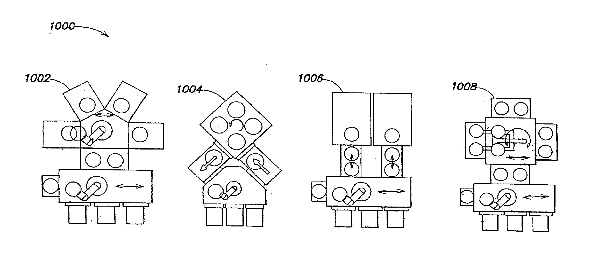
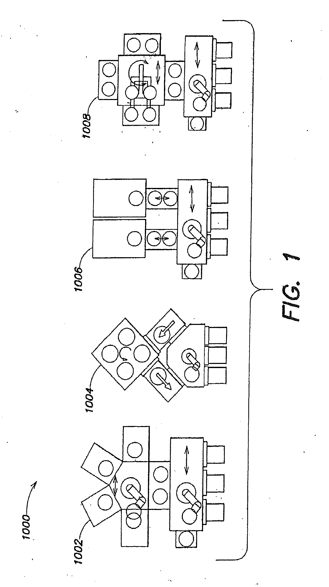
[0154]FIG. 1 shows equipment architectures 1000 for a variety of manufacturing equipment types. Each type of manufacturing equipment handles items, such as semiconductor wafers, between various processes, such as chemical vapor deposition processes, etching processes, and the like. As semiconductor manufacturing processes are typically extremely sensitive to contaminants, such as particulates and volatile organic compounds, the processes typically take place in a vacuum environment, in one or more process modules that are devoted to specific processes. Semiconductor wafers are moved by a handling system among the various processes to produce the end product, such as a chip. Various configurations 1000 exist for handling systems. A prevalent system is a cluster tool 1002, where process modules are positioned radially around a central handling system, such as a robotic arm. In other embodiments, a handling system can rotate items horizontally, such as in the embodiment 1004. An import...


PUM


Abstract

A substrate processing system including at least two vertically stacked transport chambers, each of the vertically stacked transport chambers including a plurality of openings arranged to form vertical stacks of openings configured for coupling to vertically stacked process modules, at least one of the vertically stacked transport chambers includes at least one transport chamber module arranged for coupling to another transport chamber module to form a linear transport chamber and another of the at least two stacked transport chambers including at least one transport chamber module arranged for coupling to another transport chamber module to form another linear transport chamber, and a transport robot disposed in each of the transport chamber modules, where a joint of the transport robot is locationally fixed along a linear path formed by the respective linear transport chamber.

Description

CROSS-REFERENCE TO RELATED APPLICATIONS[0001]This application is the National Stage of International Application No. PCT / IB2012 / 002688 having International Filing date, 26 Oct. 2012, which designated the United States of America, and which International Application was published under PCT Article 21 (s) as WO Publication 2013 / 072760 A2 and which claims priority from, and benefit of U.S. provisional patent application No. 61 / 551,779 filed on 26 Oct. 2011, the disclosures of which are incorporated by reference herein in their entireties.BACKGROUND[0002]1. Field[0003]The aspects of the disclosed embodiment relate to semiconductor processing systems, and specifically relates to vacuum semiconductor processing work piece handling and transportation.[0004]2. Brief Description of Related Developments[0005]Current semiconductor manufacturing equipment takes several different forms, each of which has significant drawbacks. Cluster tools, machines that arrange a group of semiconductor proces...

Claims


Application Information

Patent Timeline
IPC IPC(8): B65G47/90
CPCB65G47/901H01L21/67173H01L21/67178H01L21/67184H01L21/67196H01L21/67715H01L21/67733B65G2201/0297H01L21/67703H01L21/67742
Inventor CAVENEY, ROBERT T.
Owner BOOKS AUTOMATION US LLC
Learn More