Disordered silicon nanocomposites for photovoltaics, solar cells and light emitting devices

a technology of solar cells and silicon nanocomposites, applied in the direction of sustainable manufacturing/processing, climate sustainability, semiconductor devices, etc., can solve the problems of significant obstacles in the application of nanocrystals in light emitting devices (light emitting diodes and laser diodes), and achieve direct electrical injection of charge carriers into nanocrystals

Inactive Publication Date: 2007-11-29
ANTEOS
View PDF4 Cites 54 Cited by
  • Summary
  • Abstract
  • Description
  • Claims
  • Application Information

AI Technical Summary

Benefits of technology

[0017]It is an object of the present invention to provide intrinsic, p-type, or n-type nanocomposite layers made of disordered-amorphous or microcrystalline / nanocrystalline-silicon or their alloys and comprising semiconductor nanoparticles encapsulated into disordered silicon matrix that ensures a direct electrical contact between the disordered silicon matrix and nanoparticles.

Problems solved by technology

Applications of nanocrystals in light emitting devices (light emitting diodes and laser diodes), however, have been significantly hindered by difficulties in achieving direct electrical injection of charge carriers into nanocrystals.
All-inorganic NC devices are obviously stable under ambient atmospheric conditions, but the methods employed for semiconductor thin film growth typically rely on conditions not compatible with NCs.

Method used


Image

  • Disordered silicon nanocomposites for photovoltaics, solar cells and light emitting devices
  • Disordered silicon nanocomposites for photovoltaics, solar cells and light emitting devices
  • Disordered silicon nanocomposites for photovoltaics, solar cells and light emitting devices

Examples


Embodiment Construction

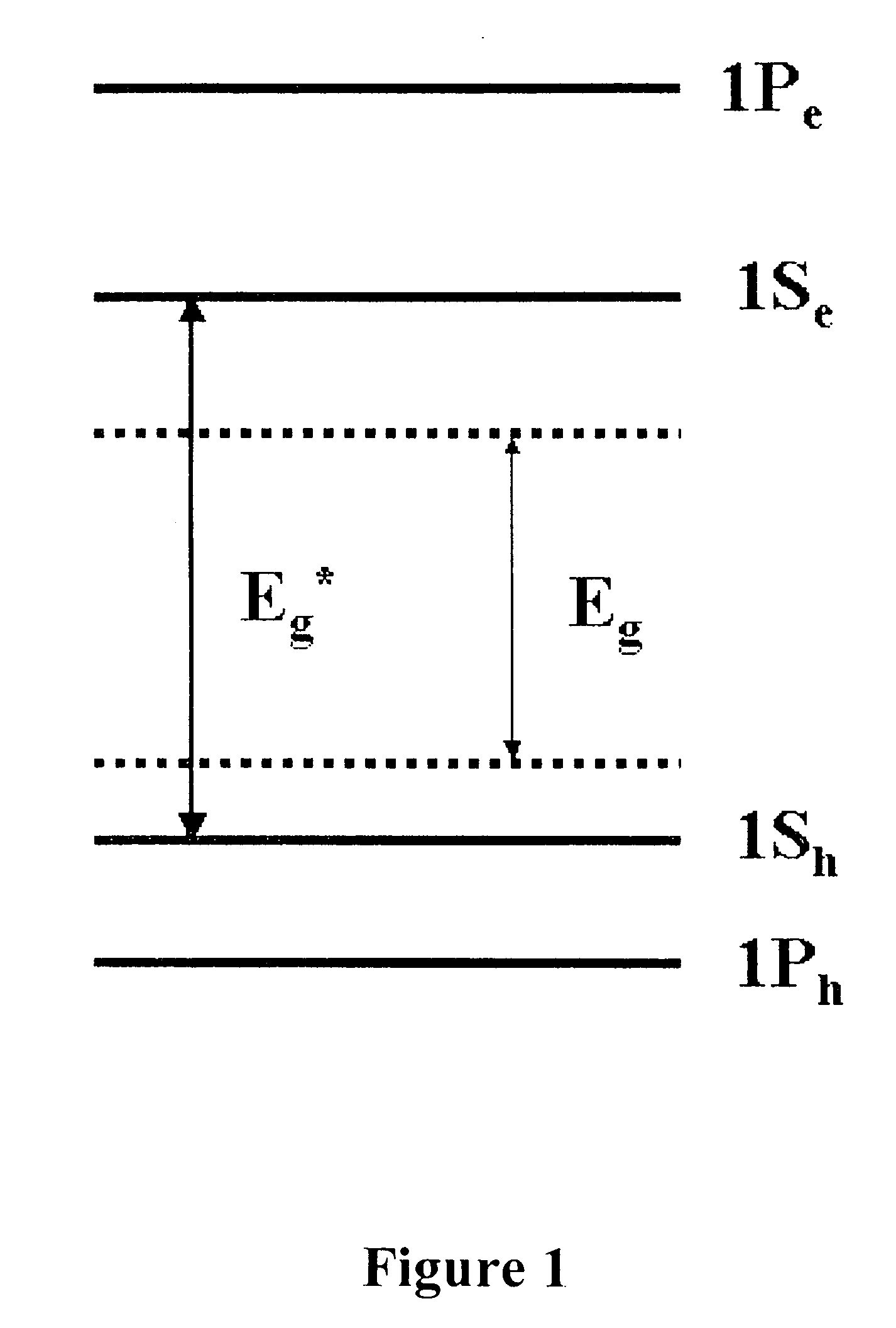
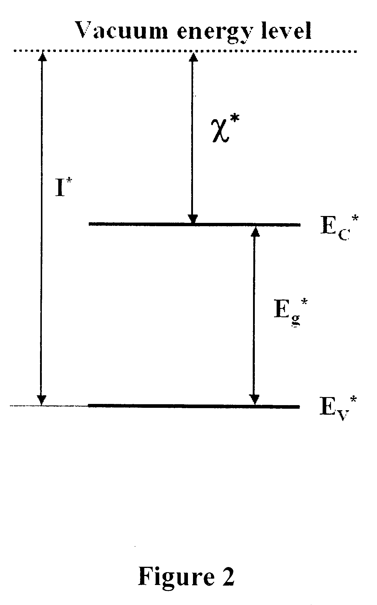
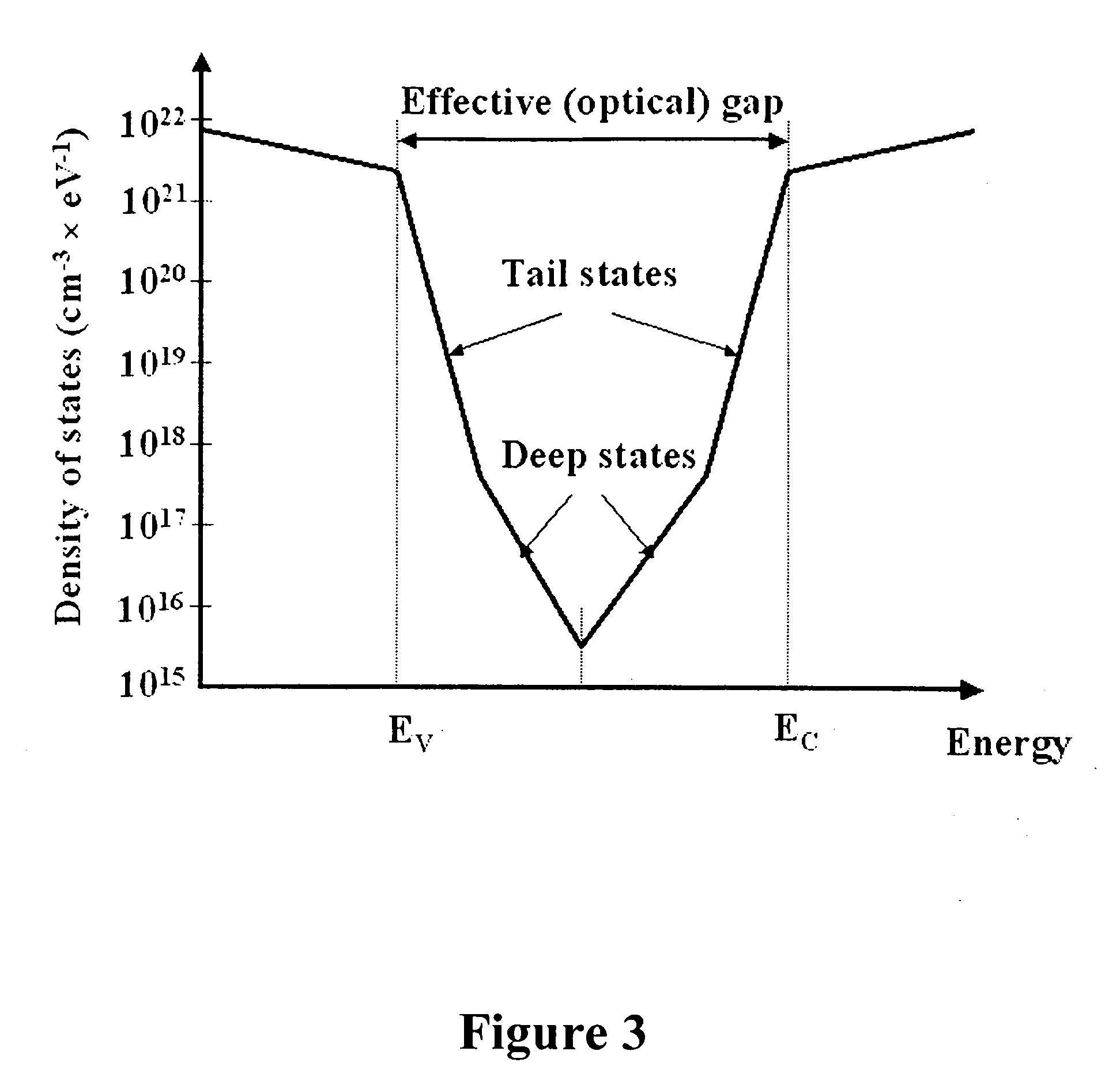
[0045]The preferred embodiments are directed to nanocomposite materials and their structures for photovoltaics, photodetectors, and light emitting devices. A key element of the preferred embodiments is a p-type, i-type or n-type layer made of disordered-amorphous or microcrystalline-silicon and comprising semiconductor nanoparticles encapsulated into the disordered silicon host. The intrinsic, p-type or n-type layers of the disordered silicon comprising nanocrystals can obviously be employed in numerous layered architectures already proposed for photovoltaic materials and light emitting devices. Apart from the nanocomposite disordered silicon layers, these structures can also comprise bulk semiconductor materials, metals, and conducting polymers. That enables development of numerous layered architectures taking advantage of nanoparticles as efficient photogenerators of electron-hole pairs for photovoltaic applications and as very attractive light emitters combining size-controlled e...


PUM

PropertyMeasurementUnit
diameteraaaaaaaaaa
diameteraaaaaaaaaa
energy bandgapaaaaaaaaaa

Abstract

The present invention describes nanocomposite material structures including layers forming p-n and p-i-n homo- and heterojunctions for application in photovoltaics, solar cells, photodetectors, and light emitting devices, comprising semiconductor nanoparticles, such as colloidal semiconductor nanocrystals, nanorods, nanowires, nanotubes, etc., wherein at least one of the layers is made of hydrogenated amorphous or microcrystalline/nanocrystalline silicon or their alloys enabling low-temperature fabrication processes preventing any degradation of physical properties of the nanoparticles.

Description

BACKGROUND OF THE INVENTION[0001]1. Field of the Invention[0002]This invention relates to nanocomposite materials and their structures, such as p-n and p-i-n homo- and hetero-junctions, comprising semiconductor nanoparticles, such as colloidal semiconductor nanocrystals, nanorods, nanowires, nanotubes, etc., incorporated into layers made of hydrogenated disordered silicon, including amorphous silicon, microcrystalline (nanocrystalline) silicon or their alloys. Incorporation of the nanoparticles into disordered silicon layers provides good electrical contact between them and disordered silicon matrix, while low-temperature deposition processes of the disordered silicon layers enables to avoid high-temperature degradation of nanoparticle properties. Preferred embodiments include nanocomposite materials with n-type and p-type doped nanoparticles, nanoparticle photovoltaic materials, solar cells, light emitting devices and photodetectors capable to operate in an extremely wide spectral ...

Claims


Application Information

Patent Timeline
Patent Type & Authority Applications(United States)
IPC IPC(8): H01L31/00
CPCH01L31/0352H01L31/072Y02E10/50H01L31/202H01L31/109Y02P70/50
Inventor KRIVOSHLYKOV, SERGEIRUPASOV, VALERY
Owner ANTEOS
Why Eureka
Try Eureka