Organic electroluminescence device

a technology of electroluminescent devices and organic el, which is applied in the direction of discharge tubes/lamp details, discharge tubes luminescnet screens, organic semiconductor devices, etc., can solve the problems of high driving voltage insufficient luminous efficiency of organic el devices, etc., to achieve small chromaticity change and high luminous efficiency

Active Publication Date: 2007-11-29
IDEMITSU KOSAN CO LTD
View PDF19 Cites 62 Cited by
  • Summary
  • Abstract
  • Description
  • Claims
  • Application Information

AI Technical Summary

Benefits of technology

[0053]According to the invention, an organic EL device can be provided which exhibits color rendition and high luminous efficiency and shows only a small change in chromaticity.

Problems solved by technology

The level of the luminous efficiency was, however, not necessarily enough.
However, the luminous efficiency of this organic EL device is not necessarily satisfactory.
However, since the affinity level of the carrier recombination region control layer is larger than the affinity level of the hole transporting blue emitting layer, the organic EL device requires a high driving voltage.
However, since holes injected from the anode are almost completely consumed by the first emitting layer, only a small number of holes are supplied to the second electron transporting emitting layer through the carrier barrier layer.
As a result, white luminous efficiency is decreased.
However, this organic EL device exhibits an insufficient luminous efficiency.
However, this organic EL device exhibits an insufficient luminous efficiency.[Patent document 1] JP-A-2003-272857[Patent document 2] JP-A-2004-235168[Patent document 3] JP-A-8-78163[Patent document 4] WO2005 / 099313[Patent document 5] WO2005 / 112518[Patent document 6] JP-A-2005-100921[Patent document 7] US-A-2006 / 0088729

Method used


Image

  • Organic electroluminescence device
  • Organic electroluminescence device
  • Organic electroluminescence device

Examples


first embodiment

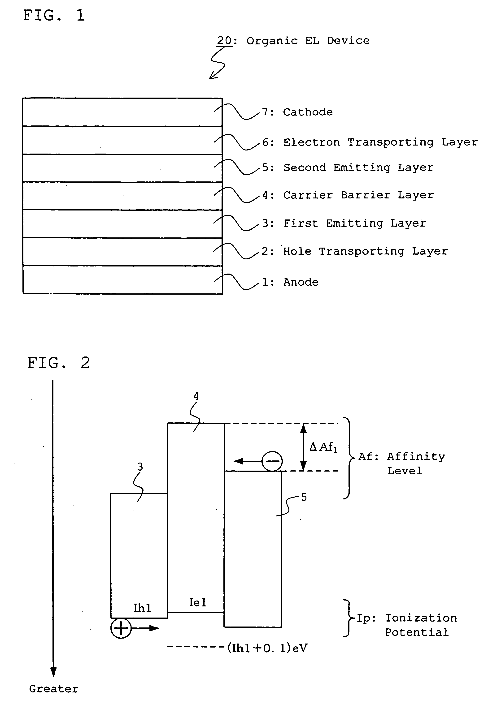
[0064]FIG. 1 is a view showing a configuration of an organic EL device according to a first embodiment of the invention.

[0065]An organic EL device 10 shown in FIG. 1 has a structure in which an anode 1, a hole transporting layer 2, a first emitting layer 3, a carrier barrier layer 4, a second emitting layer 5, an electron transporting layer 6, and a cathode 7 are stacked.

[0066]The organic EL device 10 can emit white light by allowing the first emitting layer 3 to emit red light and the second emitting layer 5 to emit blue light, for example.

[0067]In the organic EL device 10 according to this embodiment, the first emitting layer 3 on the anode 1 side is formed of a hole transporting material, and the second emitting layer 5 on the cathode 7 side is formed of an electron transporting material. This allows injection of electrons into the first emitting layer 3 and injection of holes into the second emitting layer 5 in a well-balanced manner. As a result, the recombination zone is conce...

second embodiment

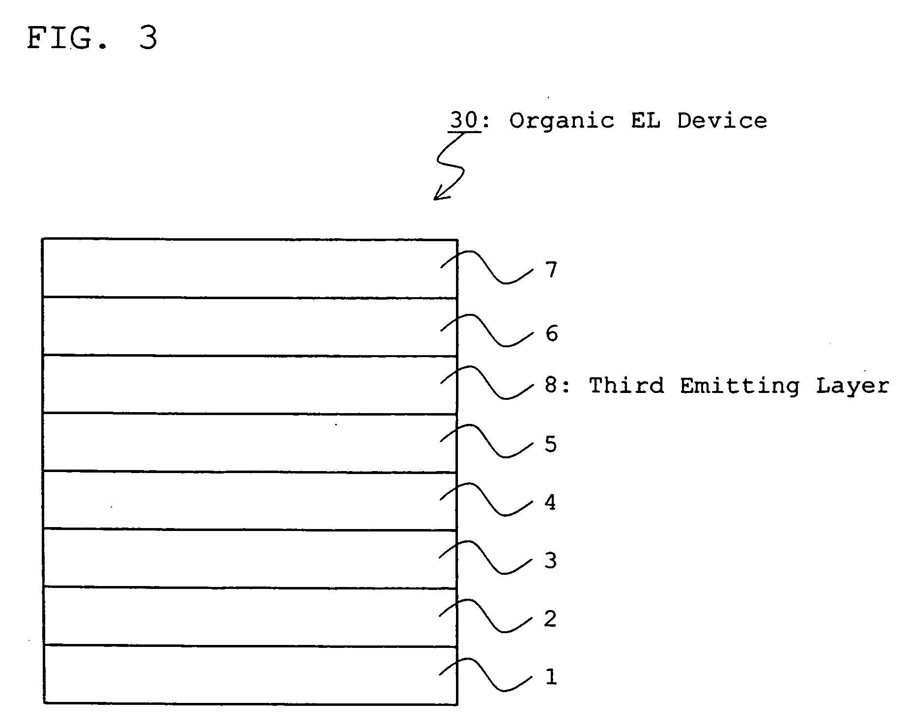
[0093]FIG. 3 is a view showing a configuration of an organic EL device according to a second embodiment of the invention.

[0094]An organic EL device 20 shown in FIG. 3 has a structure in which the anode 1, the hole transporting layer 2, the first emitting layer 3, the carrier barrier layer 4, the second emitting layer 5, a third emitting layer 8, the electron transporting layer 6, and the cathode 7 are stacked. Specifically, the organic EL device 20 has the same configuration as in the first embodiment except that the third emitting layer 8 is additionally formed. The third emitting layer 8 is formed of an electron transporting material in the same manner as the second emitting layer 5.

[0095]The organic EL device 20 can emit white light with more excellent color rendition by allowing the first emitting layer 3 to emit red light, the second emitting layer 5 to emit blue light, and the third emitting layer 8 to emit green light, for example.

[0096]In this embodiment, the first emitting ...

third embodiment

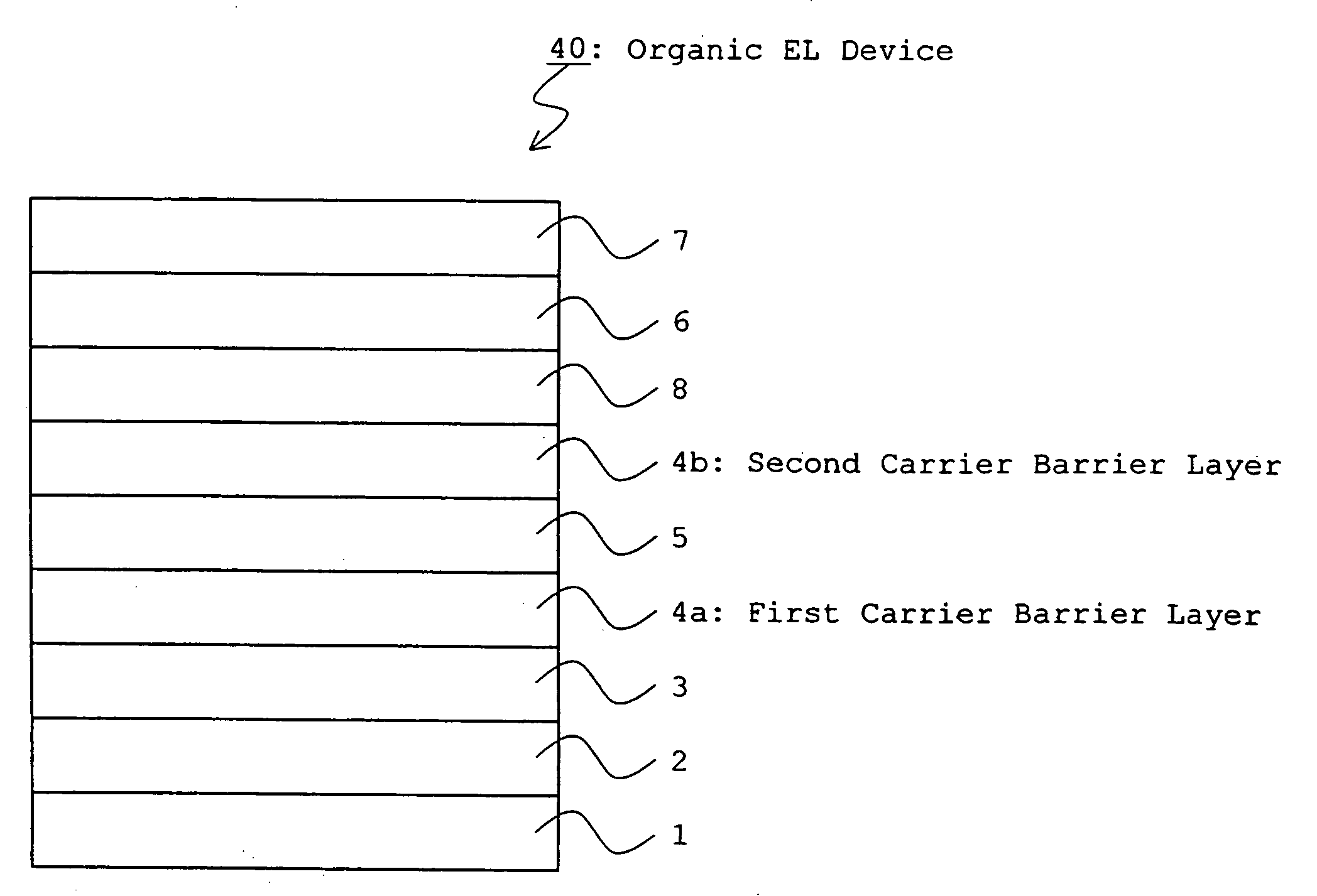
[0099]FIG. 4 is a view showing a configuration of an organic EL device according to a third embodiment of the invention. FIG. 5 is a view showing the energy levels of the first emitting layer, first carrier barrier layer, second emitting layer, second carrier barrier layer, and third emitting layer of this organic EL device.

[0100]An organic EL device 40 shown in FIG. 4 has a structure in which the anode 1, the hole transporting layer 2, the first emitting layer 3, a first carrier barrier layer 4a, the second emitting layer 5, a second carrier barrier layer 4b, the third emitting layer 8, the electron transporting layer 6, and the cathode 7 are stacked. Specifically, the organic EL device 40 has the same configuration as in the second embodiment except that the second carrier barrier layer 4b is additionally formed.

[0101]It is possible to cause the second emitting layer 5 and the third emitting layer 8 to emit light in a well-balanced manner by forming the second carrier barrier laye...


PUM


Abstract

An organic electroluminescent device (20) including an anode (1), a first emitting layer (3), a carrier barrier layer (4), a second emitting layer (5), and a cathode (7) stacked in that order. The first emitting layer (3) is formed of a hole transporting material, and the second emitting layer (5) is formed of an electron transporting material. The affinity level of the carrier barrier layer (4) is smaller than the affinity level of the second emitting layer (5) in an amount of 0.2 eV or more, and the ionization potential (Ie1) of the carrier barrier layer (4) and the ionization potential (Ih1) of the first emitting layer (3) satisfy Ie1<Ih1+0.1 (eV) (1).

Description

TECHNICAL FIELD [0001]The invention relates to an organic electroluminescent device.TECHNICAL BACKGROUND [0002]Recently, white organic electroluminescent (EL) devices are being actively developed because they can be used for a mono-color display device, a lighting application such as a back light, and a full-color display with color filters. In the case where white organic EL devices are used for lighting applications, they are required to have a high luminous efficiency, for example, which is equivalent to or more than that of fluorescent lamps.[0003]Many methods of producing white light emission by an organic EL device have been disclosed. Few of the methods produce white light with only one kind of emitting material and a single organic EL device generally uses two or three kinds of emitting materials that emit light simultaneously. In the case of using two kinds of emitting materials, a blue emitting material and a yellow-to-red emitting material, yellow-to-red being the complem...

Claims


Application Information

Patent Timeline
Patent Type & Authority Applications(United States)
IPC IPC(8): H01J1/62
CPCH01L51/0054H01L51/0056H01L2251/552H01L51/5096H01L51/5036H10K85/622H10K85/624H10K50/125H10K50/18H10K2101/30
Inventor JINDE, YUKITOSHIKUMA, HITOSHI
Owner IDEMITSU KOSAN CO LTD
Why Eureka
Try Eureka