

Unit circuit, electro-optical device, and electronic apparatus
- Summary
- Abstract
- Description
- Claims
- Application Information
AI Technical Summary
Benefits of technology
Problems solved by technology
Method used
Image

Examples
embodiment
1. Embodiment
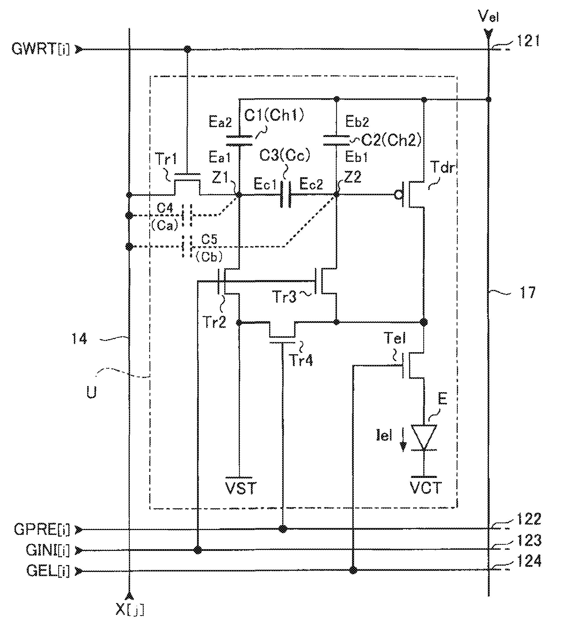
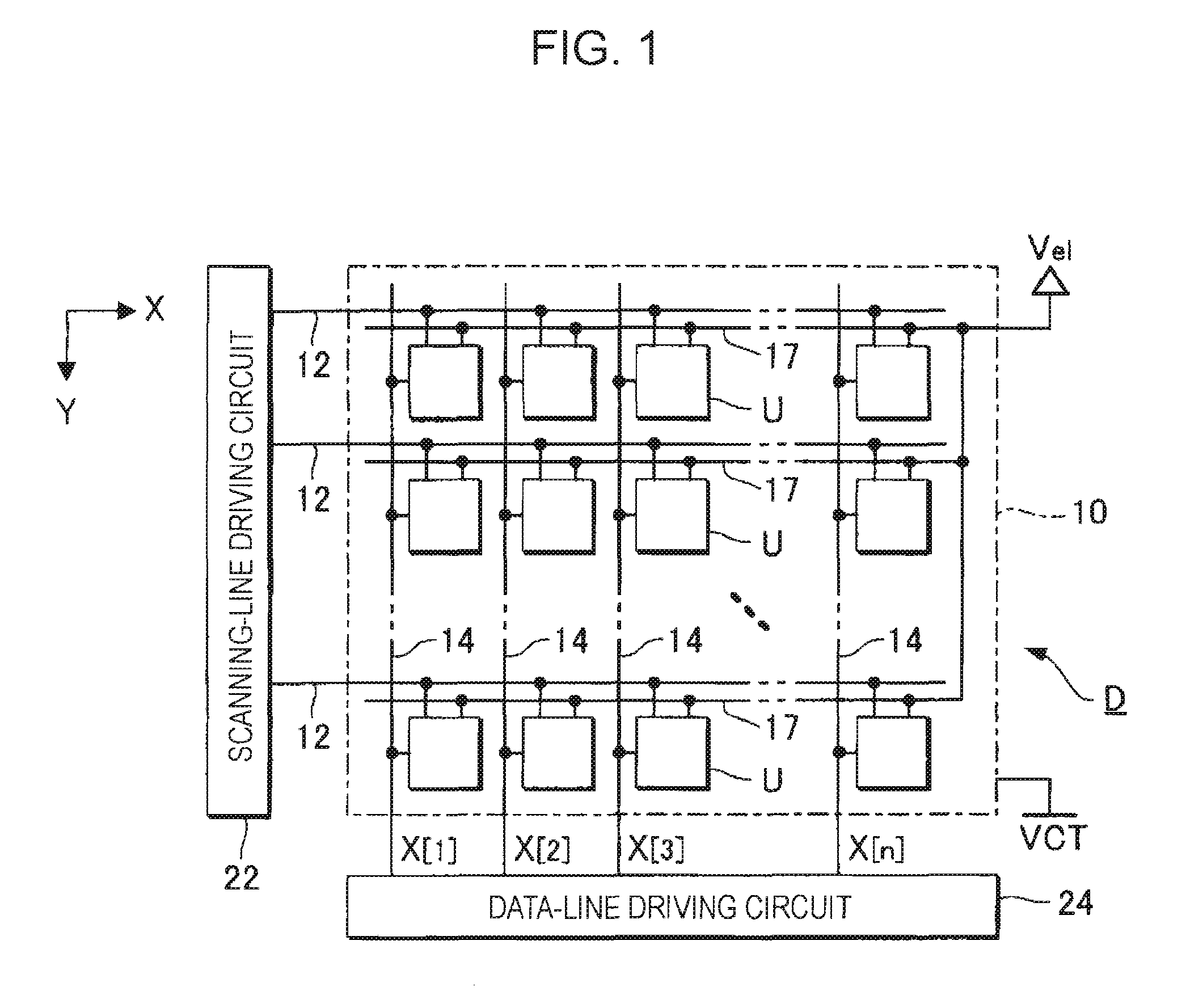
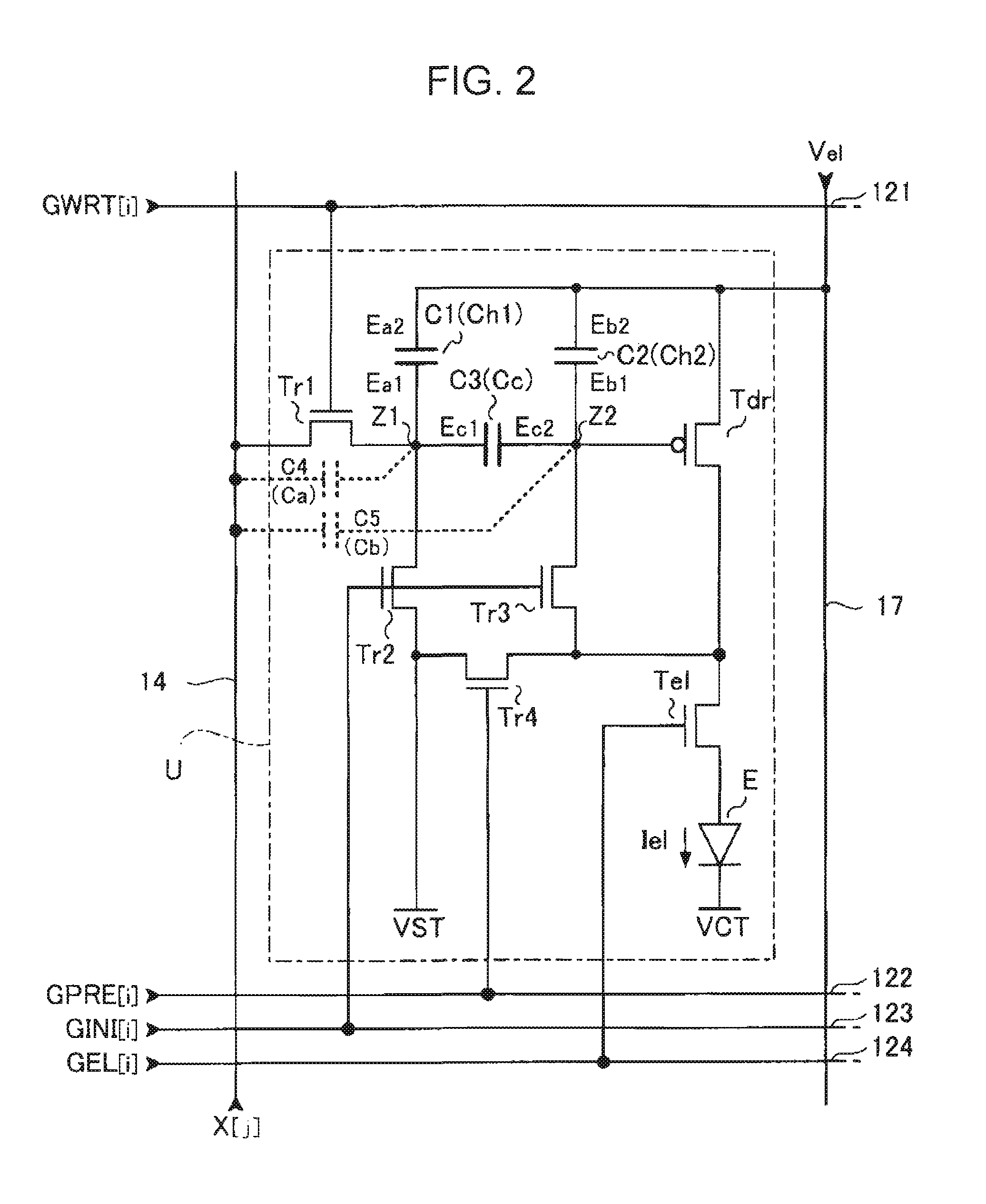
[0038]FIG. 1 is a block diagram illustrating the structure of an electronic apparatus according to an embodiment of the invention. An electronic device D illustrated in FIG. 1 is an electro-optical device (light emitting device) incorporated as an image displaying unit in one of various kinds of electronic apparatuses. The electronic device D includes an element array 10 having a plurality of unit circuits (pixel circuits) U arranged in a generally planer configuration. The electronic device D also includes a scanning-line driving circuit 22 and a data-line driving circuit 24 for driving the unit circuits U. Each of the scanning-line driving circuit 22 and data-line driving circuit 24 may be constructed of a transistor formed together with the element array 10 on a substrate or may be implemented in the form of an IC chip.
[0039]As illustrated in FIG. 1, the element array 10 is provided with m scanning lines 12 extending in the X direction and n data lines 14 extending i...
first modification
(1) First Modification
[0073]FIG. 8 illustrates a unit circuit U1. In the unit circuit U1, different signals are supplied to the gate of each of the transistors Tr2 and Tr3. In this example, a second compensation control signal GINI2[i] is supplied to the third control line 123, and a first compensation control signal GINI1[i] is supplied to a fifth control line 125. The operation of the unit circuit U1 is substantially the same as in the above-described embodiment in the initialization period P0, compensation period P1, data writing period P2, and driving period P3. As the first compensation control signal GINI1[i] and second compensation control signal GINI2[i], the compensation control signal GINI[i] described above is supplied (see FIG. 3).
[0074]Before shipping of the electronic device D, various inspections are performed. One of the inspections is to inspect a short circuit of each of the first capacitive element C1 and the third capacitive element C3. In an inspection term, the...
second modification
(2) Second Modification
[0075]FIG. 9 illustrates a unit circuit U2. The unit circuit U2 is substantially the same as the unit circuit U illustrated in FIG. 2 according to the embodiment, with the exception that the transistor Tr2 is disposed between a power-supply line that supplies the initialization potential VST and a first input terminal of the transistor Tr4. In the unit circuit U2, a supply of substantially the same signals as in the embodiment described above to the first control line 121 to the fourth control line 124 can cause the third capacitive element C3 to discharge charges stored therein in the initialization period P0, cause the second capacitive element C2 to hold the threshold voltage Vth in the compensation period P1, and cause the third capacitive element C3 to operate as a coupling capacitance and a potential corresponding to a data potential to be applied to the gate of the drive transistor Tdr and held thereby In the data writing period P2. In addition, it caus...
PUM
 Abstract
Description
Claims
Application Information