Magnetic memory device and method for fabricating the same

a memory device and magnetic technology, applied in the field of magnetic memory devices, can solve the problems of difficult to form restriction regions, difficult to reduce costs, difficult etc., and achieve the effect of small space required to form recording layers, easy formation of recording layers, and relatively easy formation

Inactive Publication Date: 2007-12-06
FUJITSU LTD
View PDF4 Cites 28 Cited by
  • Summary
  • Abstract
  • Description
  • Claims
  • Application Information

AI Technical Summary

Benefits of technology

[0017]According to the present invention, the second recording layer portion is formed above the first recording layer portion, and the end of the second recording layer portion is connected to one end of the first recording layer portion, whereby the space required to form the recording layer can be small. Besides, such recording layer can be formed relatively easily. According to the present invention, the pinning sites for restricting the motion of the domain walls are easily formed in the recording layer by photolithography. Thus, the present invention can provides a magnetic memory device and a method for fabricating the magnetic memory device which can easily realize high integration.
[0018]According to the present invention, the first recording layer portion and the second recording layer portion are arranged side by side with respect to the plane of the substrate, and the end of the first recording layer portion and the end of the second recording layer portions are connected to each other, whereby the region required to form the recording layer can be short. Thus, the present invention can provide a magnetic memory device of high integration. The present invention can also increase the degree of freedom of the layout in designing.

Problems solved by technology

However, in the technique proposed in Patent Reference 1, the recording layer in a U-shape or others is formed vertically to the substrate, which makes it difficult to form the recording layer.
It is not easy either to form the restriction regions (pining sites) for restricting the motion of the domain walls in such recording layer.
Furthermore, the technique proposed in Patent Reference 1, in which the recording layer is formed vertical to the substrate, has a very large number of fabrication steps, which makes it difficult to decrease the cost.

Method used


Image

  • Magnetic memory device and method for fabricating the same
  • Magnetic memory device and method for fabricating the same
  • Magnetic memory device and method for fabricating the same

Examples


first embodiment

A First Embodiment

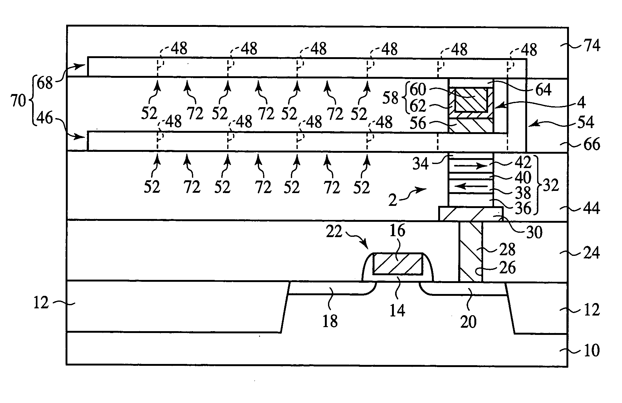
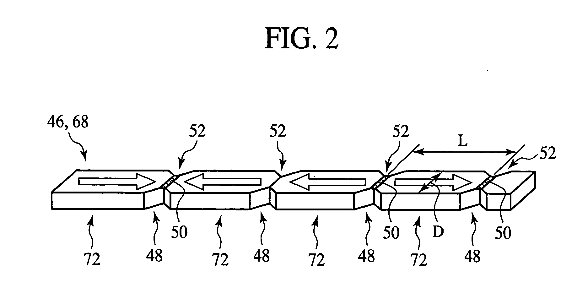
[0038]The magnetic memory device and the method for fabricating the memory device according to a first embodiment of the present invention will be explained with reference to FIGS. 1 to 13B. FIG. 1 is a sectional view of the magnetic memory device according to the present embodiment, which illustrates a structure thereof. FIG. 2 is a perspective view of the recording layers of the magnetic memory device according to the present embodiment. Hundreds to tens of thousands of recording bits can be formed in the recording layers of the magnetic memory device according to the present embodiment, but several recording bits are illustrated here.

[0039](The Magnetic Memory Device)

[0040]First, the magnetic memory device according to the present embodiment will be explained with reference to FIGS. 1 and 2.

[0041]Device isolation regions 12 for defining device regions are formed on a silicon substrate 10.

[0042]On the silicon substrate 10 with the device isolation regions 12 form...

second embodiment

A Second Embodiment

[0138]The magnetic memory device and the method for fabricating the magnetic memory device according to a second embodiment of the present invention will be explained with reference to FIGS. 14 to 19. FIG. 14 is a plan view illustrating the recording layer of the magnetic memory device according to the present embodiment. FIG. 15 is a sectional view of the magnetic memory device according to the present embodiment. Hundreds to tens of thousands of recording bits can be formed in the recording layers of the magnetic memory device according to the present embodiment, but several recording bits are illustrated here. The same members of the present embodiment as those of the magnetic memory device and the method for fabricating the magnetic memory device according to the first embodiment illustrated in FIGS. 1 to 13B are represented by the same reference numbers not to repeat or to simplify their explanation.

[0139](The Magnetic Memory Device)

[0140]The magnetic memory ...


PUM


Abstract

The magnetic memory device comprises a recording layer 70 formed linearly over a substrate 10 and having a plurality of pinning sites 52 for restricting the motion of domain walls 50 formed at a prescribed pitch and having the regions between the plural pinning sites 52 as recording bits 72. The recording layer 70 includes a first recording layer portion 46 and a second recording layer portion 68, and the second recording layer portion 68 is positioned above the first recording layer portion 46 and has one end connected to one end of the first recording layer portion 46. The second recording layer portion 68 is formed above the first recording layer portion 46, and the end of the second recording layer portion 68 is connected to one end of the first recording layer portion 46, whereby the space required to form the recording layer 70 can be small.

Description

CROSS-REFERENCE TO RELATED APPLICATION[0001]This application is based upon and claims priority of Japanese Patent Application No. 2006-151253, filed on May 31, 2006, the contents being incorporated herein by reference.BACKGROUND OF THE INVENTION[0002]The present invention relates to a magnetic memory device and a method for fabricating the magnetic memory device, more specifically, a magnetic memory device including linear recording layers and a method for fabricating the magnetic memory device.[0003]Recently, as a rewritable nonvolatile memory, the magnetic random access memory (hereinafter called “MRAM”), which magnetoresistance effect elements laid out in a matrix, is noted. The MRAM utilizes combinations of magnetization directions of two magnetic layers to store information and detects resistance changes (i.e., current or voltage changes) given when the magnetization directions of the magnetic layers are parallel with each other and anti-parallel with each other to read the sto...

Claims


Application Information

Patent Timeline
Patent Type & Authority Applications(United States)
IPC IPC(8): H01L43/00
CPCG11C11/15G11C19/0841G11C19/0808
Inventor OCHIAI, TAKAOUMEHARA, SHINJIROASHIDA, HIROSHISATO, MASASHIGESHIMIZU, YUTAKA
Owner FUJITSU LTD
Why Eureka
Try Eureka