Quantification of adsorbed molecular contaminant using thin film measurement
- Summary
- Abstract
- Description
- Claims
- Application Information
AI Technical Summary
Problems solved by technology
Method used
Image

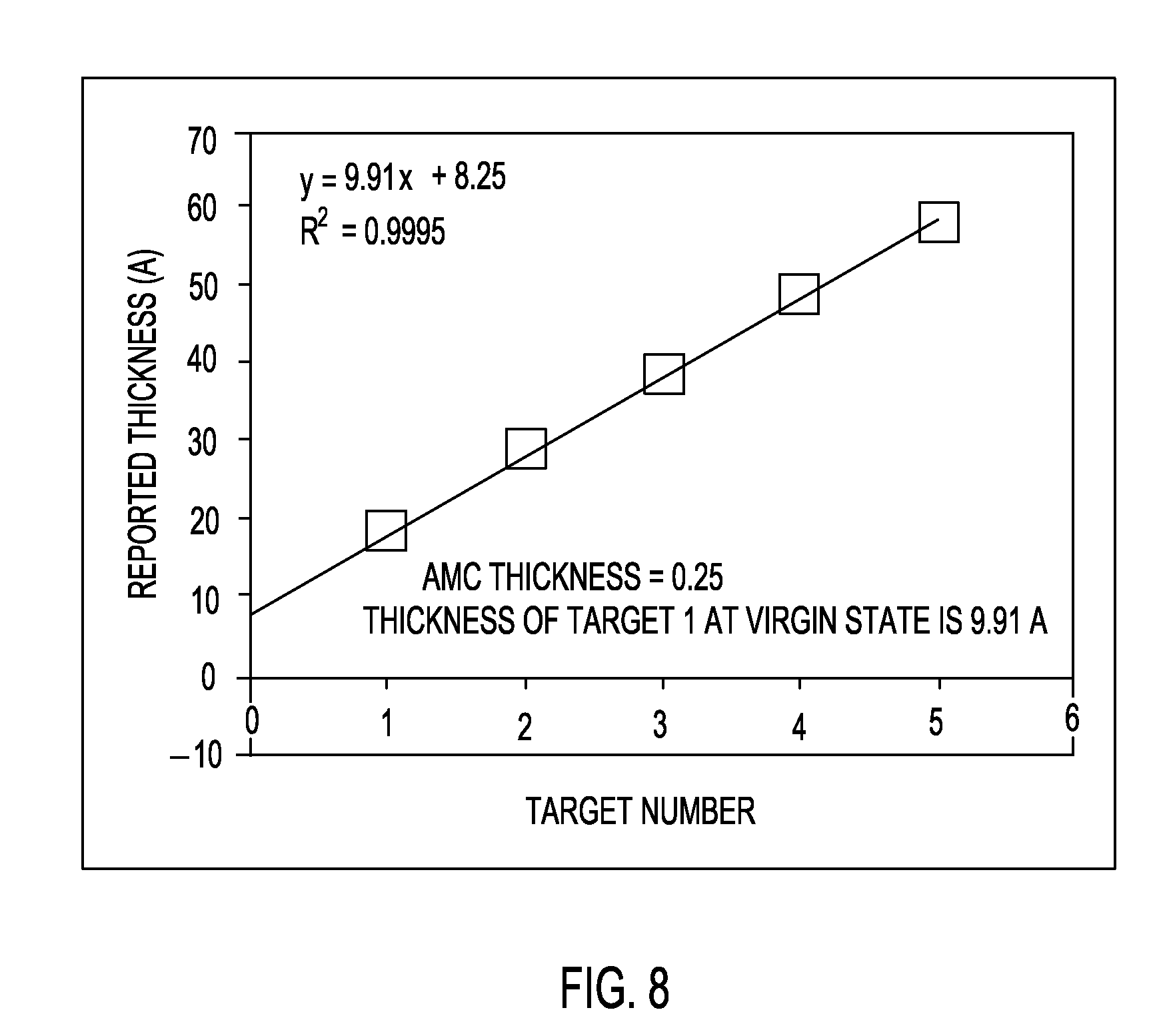
Examples
Embodiment Construction
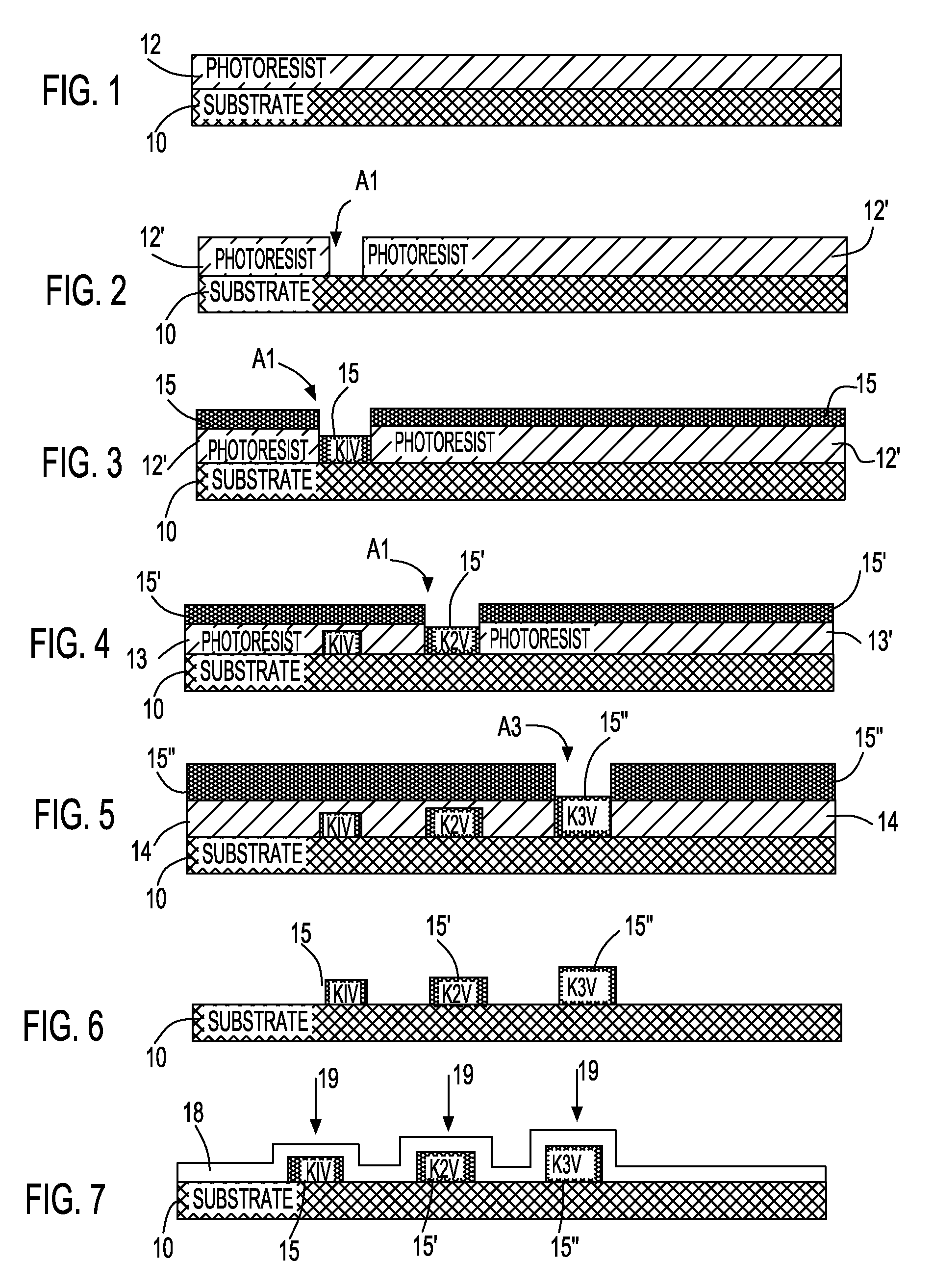
[0015]The invention, which includes a method for quantifying adsorbed molecular contamination while using a particular adsorbed molecular contaminant test structure, is disclosed in further detail within the context of the description provided below. The description provided below is understood within the context of the drawings described above. The drawings are intended for illustrative purposes, and as such are not necessarily drawn to scale.
[0016]FIG. 1 to FIG. 7 show a series of schematic cross-sectional diagrams illustrating the results of progressive stages of fabrication and use of an adsorbed molecular contaminant test structure in accordance with the preferred embodiment of the invention.
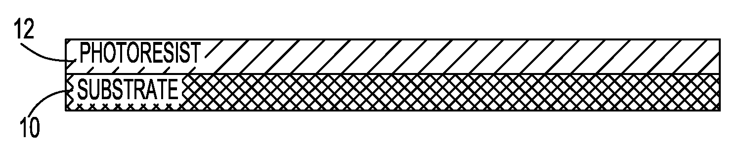
[0017]FIG. 1 shows a substrate 10. A first photoresist layer 12 is located upon the substrate 10.
[0018]The substrate 10 may comprise any of several materials. Non-limiting examples include conductor materials, semiconductor materials and dielectric materials. For convenience of use within s...
PUM
| Property | Measurement | Unit |
|---|---|---|
| thickness | aaaaa | aaaaa |
| thickness | aaaaa | aaaaa |
| thickness | aaaaa | aaaaa |
Abstract
Description
Claims
Application Information
 - R&D Engineer
- R&D Manager
- IP Professional
- Industry Leading Data Capabilities
- Powerful AI technology
- Patent DNA Extraction
Browse by: Latest US Patents, China's latest patents, Technical Efficacy Thesaurus, Application Domain, Technology Topic.
© 2024 PatSnap. All rights reserved.Legal|Privacy policy|Modern Slavery Act Transparency Statement|Sitemap