Method for Growing a Monocrystalline Tin-Containing Semiconductor Material

a monocrystalline tin-containing, semiconductor technology, applied in the direction of crystal growth process, photovoltaic energy generation, electrical equipment, etc., can solve the problems of low throughput, high cost, and limited substitutional sn, and achieve the effect of reducing the cost of snd

Inactive Publication Date: 2014-01-23
INTERUNIVERSITAIR MICRO ELECTRONICS CENT (IMEC VZW) +1
View PDF6 Cites 388 Cited by
  • Summary
  • Abstract
  • Description
  • Claims
  • Application Information

AI Technical Summary

Benefits of technology

[0006]It is an object of embodiments of the present invention to provide an efficient method for providing Sn-containing semiconductor material onto a substrate.
[0008]In a first aspect, the present invention provides a method for depositing a monocrystalline Sn-containing semiconductor material on a substrate. The method comprises providing a semiconductor material precursor, a Sn precursor and a carrier gas in a chemical vapor deposition (CVD) reactor, and epitaxially growing the Sn-containing semiconductor material on the substrate. The Sn precursor comprises tin tetrachloride (SnCl4). It is an advantage of embodiments of the present invention that an efficient method is provided for providing Sn-containing semiconductor material onto a substrate.
[0013]In particular embodiments, especially for example in case of the selected total pressure in the CVD reactor being atmospheric pressure, a ratio between SnCl4 flow and Ge2H6 flow may be equal to or lower than 0.2, for example between 0.2 and 0.1, or even below 0.1. In alternative embodiments, where the pressure in the reactor is selected below atmospheric pressure, for example about 100 Torr, a ratio between SnCl4 flow and Ge2H6 flow may be closer to 1, e.g. between 0.8 and 1.0. The latter gives better Sn-containing material properties.
[0024]It is an advantage of embodiments of the present invention that SnCl4 may be used as a Sn precursor, which is stable and commercially available at relatively low cost. Furthermore, it is an advantage of embodiments of the present invention that SnCl4 used as precursor is a low temperature Sn precursor, e.g. it may be used at temperatures below 650° C., for example even lower than 500° C. Hence a method according to embodiments of the present invention may be used for low temperature deposition of Sn-containing semiconductor materials.
[0025]It is an advantage of embodiments of the present invention that CVD may be used as the deposition process, which is a relatively simple and inexpensive deposition technique.

Problems solved by technology

Although it is possible to deposit GeSn with high non-substitutional Sn content, the percentage of substitutional Sn is limited as the solubility limit is very low.
For example, it is known that GeSn with a Sn content higher than 20 at % can be grown by Molecular Beam Epitaxy (MBE), which is a low throughput and expensive technique and therefore not advantageous for industrial applications.
However, SnD4 is a very unstable and expensive precursor, not suited for high volume manufacturing.

Method used


Image

  • Method for Growing a Monocrystalline Tin-Containing Semiconductor Material
  • Method for Growing a Monocrystalline Tin-Containing Semiconductor Material
  • Method for Growing a Monocrystalline Tin-Containing Semiconductor Material

Examples


examples

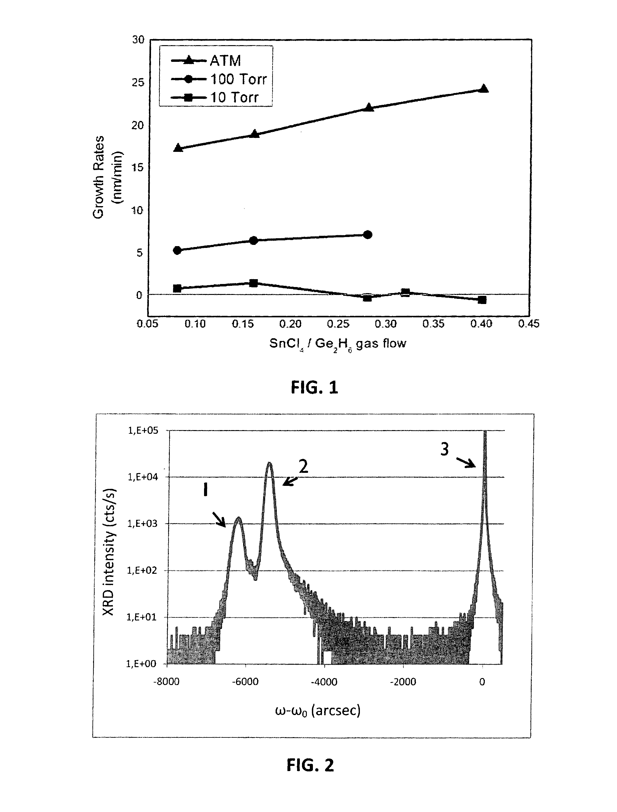
[0076]FIG. 1 shows the growth rate of epitaxially grown GeSn as function of the ratio (SnCl4 flow) / (Ge2H6 flow) at 320° C. and different total pressures in the reactor (reduced pressure: 10 Torr, 100 Torr; atmospheric pressure-ATM).

[0077]In this first example illustrated in FIG. 1 the GeSn layer is overlying and in contact with a Ge buffer layer having a thickness of 50 nm on a silicon substrate. As said before, diluted digermane with a dilution of 1% in H2 is supplied to the CVD reactor. In this example 250 sccm Ge2H6 was employed and the ratio was varied by modifying the SnCl4 flow between 20 sccm and 100 sccm. By modifying the SnCl4 flow and the total pressure in the reactor for a selected value of the Ge2H6 flow, different partial pressures of the Sn precursor in the reactor are created. It can be seen that growth rates of the GeSn layer are higher at higher pressures in the CVD reactor. Furthermore, growth rates of the GeSn layer increase with increasing SnCl4 / Ge2H6 ratio, exce...


PUM

PropertyMeasurementUnit
temperatureaaaaaaaaaa
temperaturesaaaaaaaaaa

Abstract

Disclosed are methods for growing Sn-containing semiconductor materials. In some embodiments, an example method includes providing a substrate in a chemical vapor deposition (CVD) reactor, and providing a semiconductor material precursor, a Sn precursor, and a carrier gas in the CVD reactor. The method further includes epitaxially growing a Sn-containing semiconductor material on the substrate, where the Sn precursor comprises tin tetrachloride (SnCl4). The semiconductor material precursor may be, for example, digermane, trigermane, higher-order germanium precursors, or a combination thereof. Alternatively, the semiconductor material precursor may be a silicon precursor.

Description

FIELD OF THE INVENTION[0001]The present invention relates to methods for manufacturing semiconductor material, more particularly to methods for providing monocrystalline semiconductor material, in particular tin-containing semiconductor material like tin germanides (GeSn) and tin silicon-germanides (SiGeSn), onto a substrate, and to layers and stacks of layers thus obtained. In particular the present invention also relates to the use of tin tetrachloride (SnCl4) as Sn-precursor for chemical vapor deposition of Sn comprising semiconductor materials.BACKGROUND OF THE INVENTION[0002]There is a growing interest in tin-containing semiconductor materials like tin germanides (GeSn) and tin silicon-germanides (SiGeSn) for many applications, such as high mobility channel and strain engineering for advanced microelectronic devices, direct bandgap Group IV materials for photonic devices or SiGeSn alloys for photovoltaic devices.[0003]Tin (Sn) has very low equilibrium solubility in Ge (less tha...

Claims


Application Information

Patent Timeline
Patent Type & Authority Applications(United States)
IPC IPC(8): H01L21/02
CPCH01L21/0262H01L21/0245H01L21/02535B33Y80/00H01L21/02532H01L31/02H01L31/048H01L31/055Y02E10/52
Inventor VINCENT, BENJAMINGENCARELLI, FEDERICALOO, ROGERCAYMAX, MATTY
Owner INTERUNIVERSITAIR MICRO ELECTRONICS CENT (IMEC VZW)
Why Eureka
Try Eureka