Compositions and methods for making silicon containing films

Active Publication Date: 2015-01-15
VERSUM MATERIALS US LLC
View PDF5 Cites 280 Cited by
  • Summary
  • Abstract
  • Description
  • Claims
  • Application Information

AI Technical Summary

Benefits of technology

The patent describes methods for depositing silicon-containing films on various surfaces, including thin film transistors, using different precursors and deposition techniques. The resulting films have a thickness ranging from 2 nm to 200 nm and a density of about 2.2 g / cm3 or greater. The methods can be carried out at low temperatures and can be used in various industrial applications such as the semiconductor industry. The technical effects of this patent include the ability to deposit thin, high-quality silicon-containing films on various surfaces using various techniques.

Problems solved by technology

However, the quality of these films are poorer.
The performance of these films under thermal and / or electrical stress (e.g. leakage current and breakdown voltage after annealing or the flatband voltage shift under Bias Temperature Stressing) is correspondingly worse.
IGZO materials have a temperature limitation of <350° C. Novel gate metals may also have temperature limitations.
Furthermore, it is desirable to further lower the processing temperature to <200° C. for plastic substrates, the PECVD films deposited from standard precursors such as silane or TEOS cannot balance all the requirements such as density, electrical quality and conformality.
Thus, it is inferred from the findings in He et al. that thinner films would be of poorer quality than thicker films.
This problem is especially critical when a lower deposition temperature is needed.
In certain instances, thinner films will have higher throughput and decrease the cycle time of the production process.
However, practical considerations such as film leakage current and ability to deposit pin-hole free dielectrics dictate that thicker films need to be used.

Method used


Image

  • Compositions and methods for making silicon containing films
  • Compositions and methods for making silicon containing films
  • Compositions and methods for making silicon containing films

Examples


example 1

Deposition of Diethylsilane (2ES) and Triethylsilane (3ES) at Deposition Temperatures of 200° C., 250° C., 300° C., 350° C., and 400° C.

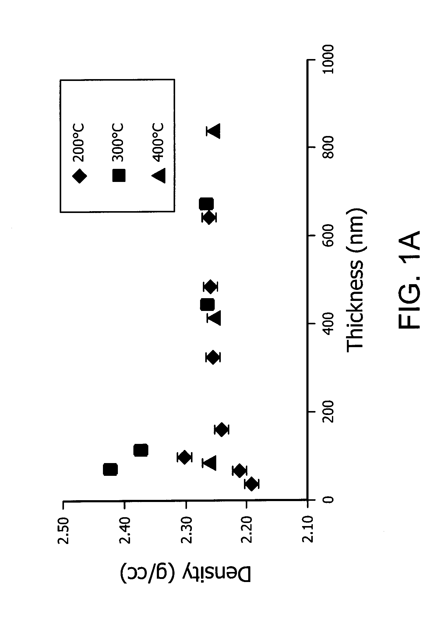
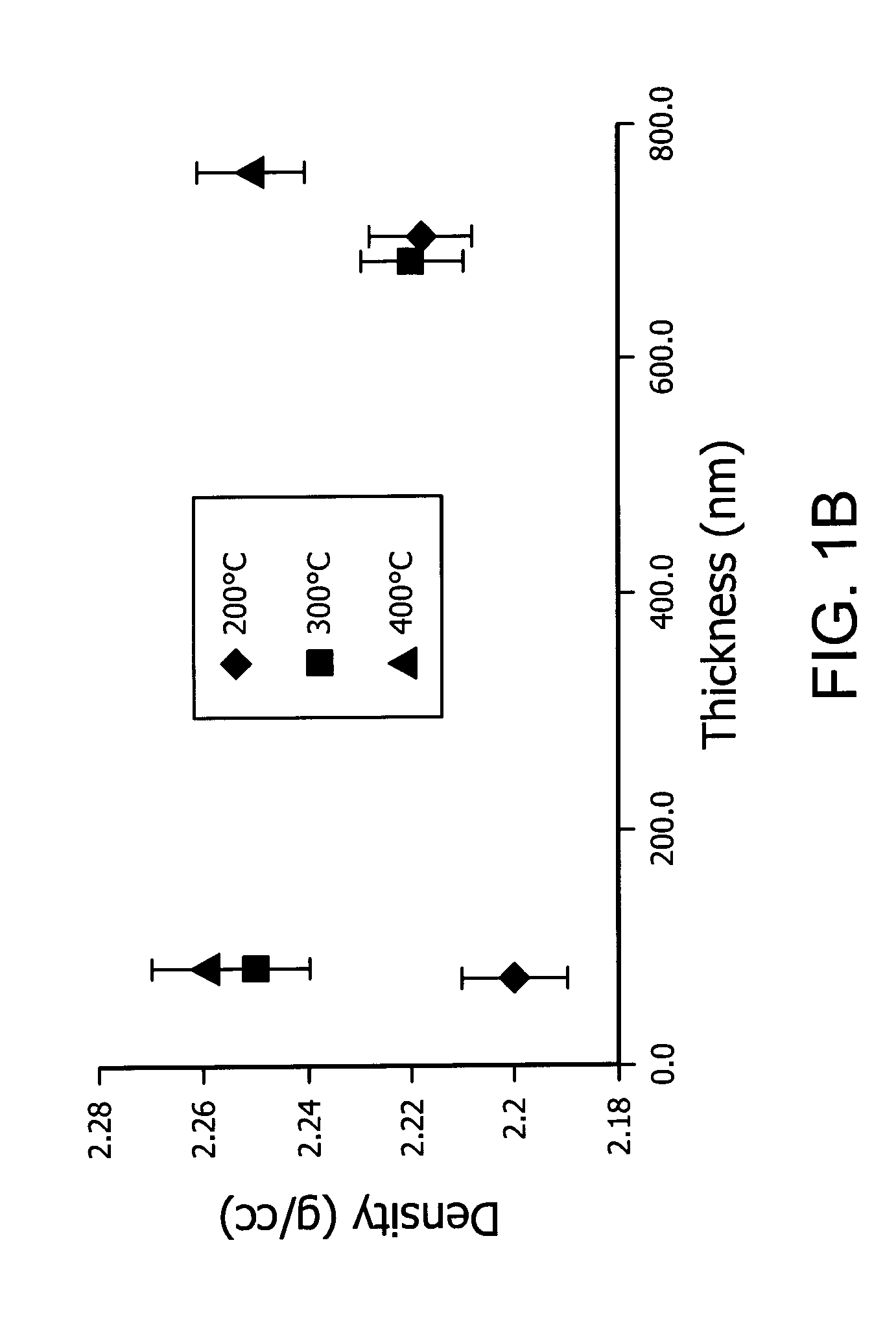
[0089]Silicon oxide films were deposited from the silicon precursors 2ES and 3ES SiO2 films were deposited at different temperature and process conditions using the general deposition conditions described above. BL-1 and BL-2 conditions are identical except for precursor flow. While BL-1 process has the highest deposition rate due to higher precursor flow, it is not the most important criterion for gate insulation layers. BL-3 is a lower pressure condition and generally gives poorer films. A comparison of same amount of Si-feed between precursors was used to understand whether a truly better quality film can be produced. As seen in FIGS. 1A and 2A, generally higher densities are obtained for films >200 nm with BL-2 process (>2.2 g / cc) and FIG. 1B, 2B; slightly lower densities were obtained with BL-3 process (˜2.2 g / cc). The BL-1 process conditions w...

example 2

Comparison of Silicon Oxide Films Deposited Using BL2 Process Condition and Tetraethoxysilane (TEOS) vs. Diethysilane (2ES)

[0095]SiO2 films were deposited using the process conditions described above in the general deposition conditions and in Table 1. In FIGS. 1C and 1D, TEOS deposited silicon oxide films having different thicknesses were deposited at the same BL-2 and BL-3 process conditions described above in Table 1. Referring to FIG. 1C, compared to the 2ES and 3ES films deposited using BL-2 at identical deposition temperatures (see FIG. 1A and FIG. 2A), at lower deposition temperatures such as 200° C., the TEOS-deposited films generally had lower density than the 2ES or 3ES films. A similar effect was observed when comparing the data in FIG. 1D with the data for the 2ES films and 3ES films in FIGS. 1B and 2B) for the same deposition temperatures. The 2ES and 3ES films generally exhibited equal or higher density for the thinner films. In general, the density of TEOS film drops ...

example 3

Deposition of Thin SiO2 Films Using 3ES with High Density and Electric Properties

[0102]Process conditions for the 3ES silicon oxide films were screened using a design of experiment (DOE) methodology summarized below: precursor flow from 10 to 200 sccm; O2 / He flow from 100 to 1000 sccm, pressure from 0.75 to 10 torr; Low-frequency (LF) power 0 to 100 W; and deposition temperature ranged from 25 to 350° C. The DOE experiments were used to determine what process parameters produced the optimal film for use as a gate insulating layer in a display device.

[0103]SiO2 films were deposited using the precursor 3ES at even lower deposition temperatures, such as 100° C., 125° C. and 150° C. then described above in the previous examples. By optimizing the process parameters, such as precursor flow, chamber pressure and power density, high density and thin SiO2 films are obtained. Table 2 shows a summary of the three process conditions used for 3ES film deposited at different temperatures 100° C....


PUM

PropertyMeasurementUnit
Temperatureaaaaaaaaaa

Abstract

Described herein are low temperature processed high quality silicon containing films. Also disclosed are methods of forming silicon containing films at low temperatures. In one aspect, there are provided silicon-containing film having a thickness of about 2 nm to about 200 nm and a density of about 2.2 g / cm3 or greater wherein the silicon-containing thin film is deposited by a deposition process selected from a group consisting of chemical vapor deposition (CVD), plasma enhanced chemical vapor deposition (PECVD), cyclic chemical vapor deposition (CCVD), plasma enhanced cyclic chemical vapor deposition (PECCVD, atomic layer deposition (ALD), and plasma enhanced atomic layer deposition (PEALD), and the vapor deposition is conducted at one or more temperatures ranging from about 25° C. to about 400° C. using an alkylsilane precursor selected from the group consisting of diethylsilane, triethylsilane, and combinations thereof.

Description

CROSS REFERENCE TO RELATED APPLICATIONS[0001]This patent application claims the priority benefit of U.S. Provisional Patent Application Ser. No. 61 / 608,955 filed Mar. 9, 2012.BACKGROUND OF THE INVENTION[0002]Disclosed herein are methods and compositions to prepare silicon-containing films, such as but not limited to, stoichiometric or non-stoichiometric silicon oxide or silicon dioxide (SiO2) films, for use in various electronic applications.[0003]Thin films of silicon oxide are commonly used as dielectrics in semiconductor manufacturing because of their dielectric properties. In the manufacturing of silicon-based semiconductor devices, silicon oxide films can be used as gate insulation layers, diffusion masks, sidewall spacers, hard mask, anti-reflection coating, passivation and encapsulation, and a variety of other uses. Silicon oxide films are also becoming increasingly important for passivation of other compound semiconductor devices.[0004]Other elements besides silica and oxyge...

Claims


Application Information

Patent Timeline
IPC IPC(8): H01L21/02H01L29/51
CPCH01L21/02164H01L21/02271H01L21/0228H01L21/02208H01L21/02274H01L21/443H01L29/7869H01L29/51C23C16/401C23C16/505H01L29/78651C23C16/402H01L29/4908
Inventor MALLIKARJUNAN, ANUPAMAJIHNSON, ANDREW DAVIDWANG, MEILIANGVRTIS, RAYMOND NICHOLASHAN, BINGLEI, XINJIANO'NEILL, MARK LEONARD
Owner VERSUM MATERIALS US LLC
Why Eureka
Try Eureka